Everything up to this point lived in software. The FPGA code ran in ModelSim and Verilator. The key layout existed as a C# mockup. The arithmetic engine was C++. Perfectly useful, but none of it had a physical key you could press.
That changed with the first PCB order.
From Schematic to Board
The first hardware goal was simple: a board with the keypad matrix and the OLED display, connected to the EP2C5 development board by a 40-pin ribbon cable. No FPGA on this board, no power supply, no battery. Just switches and a display connector, and a keypad I could actually type on.
The tool I used for the design was EasyEDA, a web-based PCB editor that runs in a browser with no installation. It is not Eagle or KiCad in terms of features, but for a simple board it is more than adequate. I recommend it if you order from JLCPCB: the two are tightly integrated and share a parts catalog.
The keypad is made of 35 tactile switches arranged in seven rows and five columns. Press a key and it connects a row line to a column line. The FPGA scans each column in turn, drives it low, and reads which row lines respond. Pull-up resistors on the row lines keep them high when no key is pressed.
The OLED is a Newhaven NHD-0216AW: a 2×16 character module with an HD44780-compatible parallel interface. Eight data lines, RS, and E. The same interface that Hitachi introduced in 1987 for LCD panels, designed to connect cleanly to the Intel MCS-51 bus, and cloned by every character display manufacturer ever since. The fact that a modern OLED module from 2021 answers to commands designed for a chip from 1987 is either a tribute to good interface design or a remarkable failure to move on, depending on your perspective. Either way, it meant the driver code was straightforward.
The PCB layout is mostly routing. EasyEDA’s autorouter handles most of it; the manual cleanup is mainly making sure the traces look clean and the silkscreen labels are legible.
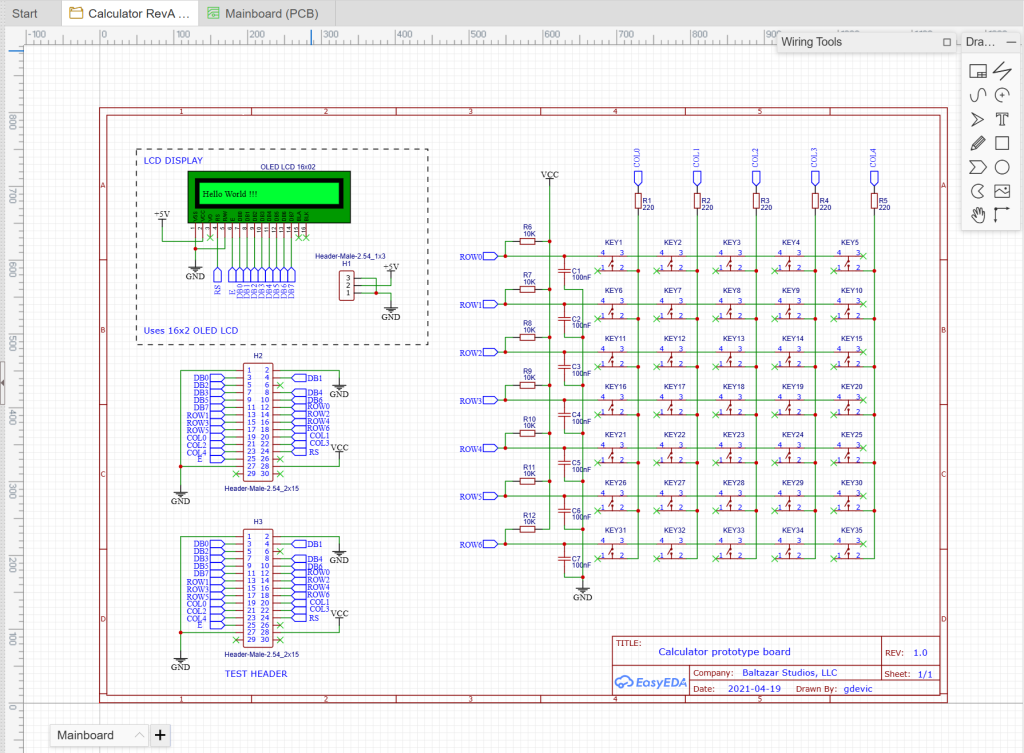
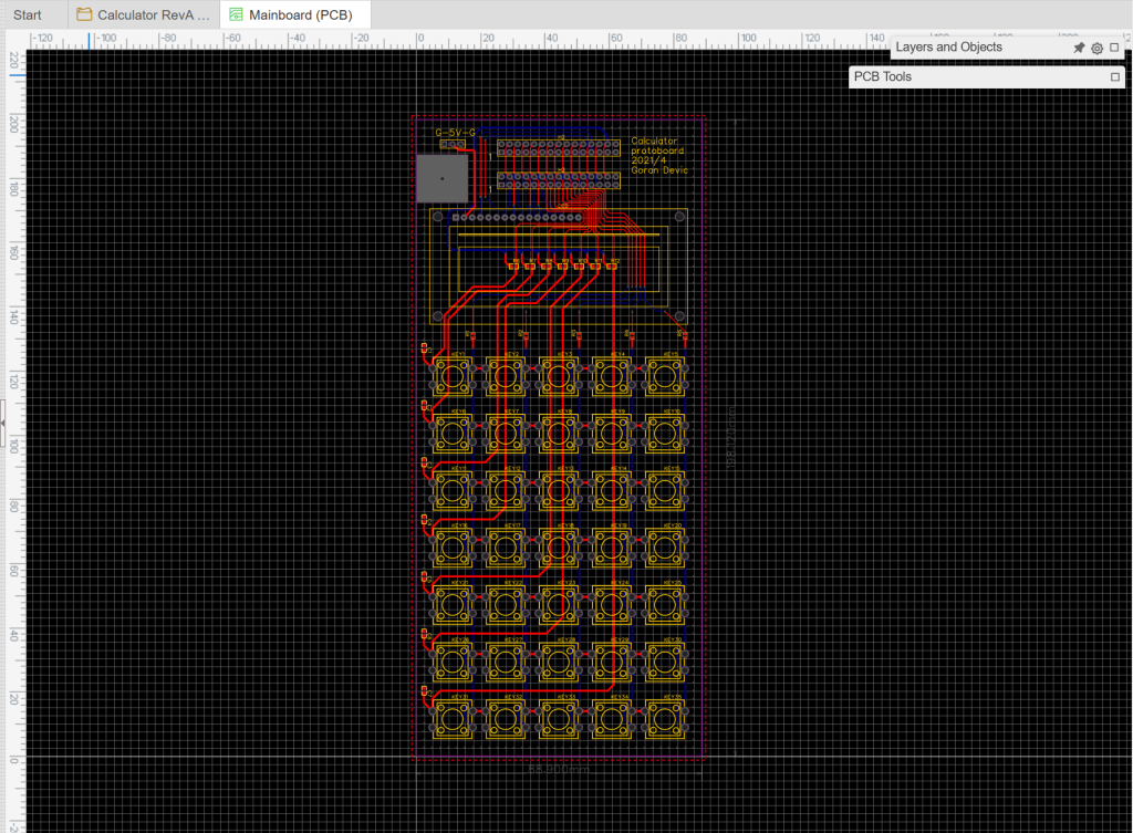
The PCB layout. The switch footprints fill most of the board; the OLED sits at the top.
Ordering from JLCPCB
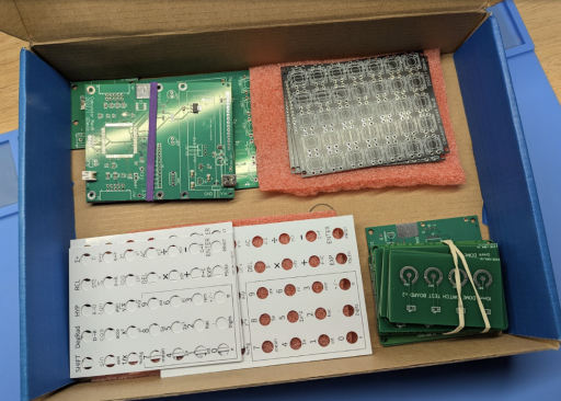
JLCPCB is a PCB manufacturer based in Shenzhen. They specialize in small prototype runs: five boards is their standard minimum, at prices that were implausible ten years ago. Five two-layer boards of this size cost roughly $2 plus shipping, delivered in about two weeks. For anyone who has ever waited six weeks and paid $50 per board at a western manufacturer, the current state of PCB prototyping is startling. (I am not sponsored by them, or by anyone, for that matter, so those are my personal experiences)
The ordering workflow from EasyEDA is direct: click “Generate Gerber” to export the standard manufacturing files, then “Order at JLCPCB” to send them. The JLCPCB site shows a 3D preview of the board before you confirm. The main choices are board dimensions, layer count (two for almost everything), surface finish (HASL is fine for prototypes), and whether you want parts assembled.
For Rev A I ordered boards only, no assembly. The component count was low enough that hand-soldering everything was faster than setting up an assembly order, and it gave me direct control over component placement. The switches and OLED went on by hand.
JLCPCB also offers SMD assembly at reasonable prices for larger component counts. The process: select “PCB+Assembly” at checkout, upload a BOM and CPL (component placement) file, and they source the parts from LCSC (their affiliated parts distributor) and place them. Parts that cannot be assembled are flagged; you source and solder those yourself. The minimum per-line quantity for assembly orders is lower than for LCSC direct orders, which is useful when you only need one of a specific component.
Total cost for five boards plus parts (switches, OLED, resistors, connectors): approximately $30 including shipping. (Note: that was in 2021. At this time, and with tariffs, the prices are much higher)
Connecting the Two Boards
The assembled keypad board connects to the EP2C5 development board by a standard 40-pin IDC ribbon cable; the same type used for IDE hard drives. The IDC (Insulation-Displacement Contact) connector pierces through the wire insulation without stripping it, cold-welding directly to the copper conductor to form a tight connection — cheap and quite reliable. One board provides the FPGA, the clock, and the JTAG programming interface. The other provides the keypad and display. The ribbon cable carries power, ground, and the GPIO signals between them.
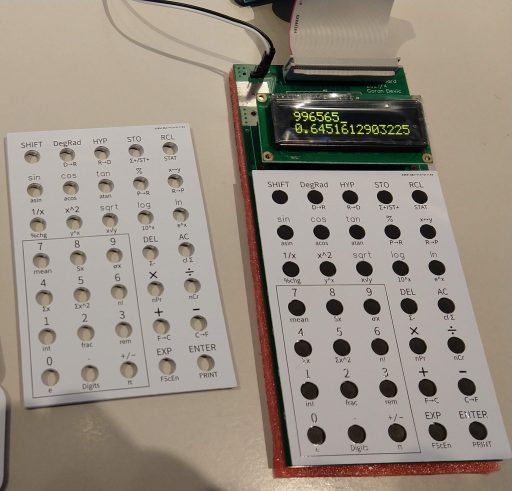
This two-board approach is a classic prototype strategy: keep the known-good commercial module untouched, attach the new custom work beside it, and connect them with a well-understood interface. If something goes wrong, the problem is almost certainly on the new board.
Getting It to Work
The keypad scanner was the second piece of Verilog to run on real hardware: drive each column pin low in seperate sequence, read the row pins, debounce, report key codes.
A mechanical tactile switch bounces for anywhere from 1ms to 20ms depending on the switch model and how hard it is pressed. Too short a debounce window and you register phantom keypresses; too long and the calculator feels sluggish. I connected the oscilloscope to a row pin and measured the actual bounce duration for the specific switches I used (Cherry-equivalent 6mm tactiles). The result was clean: well under 5ms, so I set the debounce threshold accordingly.
The pull-up resistor values needed some educated guessing. The row lines need to be high when no key is pressed, but not so strongly pulled up that a pressed key cannot pull the row down to the driven column’s low level. The values I had calculated on paper worked first try, which was satisfying.
The OLED initialization sequence requires specific delays between commands: the controller’s internal reset is slow, and the host has to wait. If you get the timing wrong, the display initializes partialy or not at all. I stepped through the sequence in ModelSim before touching hardware, so it worked on the first attempt.
What Rev A Established
Rev A ran for several months before Rev B was designed. In that time, every peripheral was characterized:
- Keypad scanner debounce timing verified on real hardware
- OLED initialization sequence confirmed
- Specific switch model and pull-up resistor values locked in
- Pin assignments between the ribbon cable and the FPGA GPIOs documented in the Quartus
.qsffile
Simulation tells you the logic is correct. Hardware tells you the timing works, and the parts behave as the datasheet says they do. The ribbon cable was fragile: two boards were unwieldy. There was no battery and no enclosure. The next step was to put everything on one board and make it something you could actually carry.
Post 6 covers the CPU design — the instruction set and microarchitecture. Post 7 is the microcode that runs on it. The journey from two boards to one finished device is Post 8.