This is the longest post because it is a central piece of this project, everything revolves around the CPU.
Why Not Just Use an Existing CPU?
The obvious objection to designing a custom CPU is: why bother? There are plenty of small, well-understood processors and cheap microcontrollers that could run the calculator firmware. Zilog Z80 is not hard to implement in an FPGA, as I already have done one (the A-Z80 project sitting on my GitHub). A 6502 would also work. A small, embedded RISC could also do a wonderful job.
The honest answer is that it would not be as interesting since it has been done many times before. But there are also other (more convenient) reasons.
Our calculator is built around BCD (binary-coded decimal), where every decimal digit lives in its own 4-bit nibble. That is the right choice for a decimal calculator, and it shapes everything downstream. A Z80 (and other off-the-shelf CPUs) operates on bytes. Indexing into a 16-nibble mantissa register with a byte-oriented processor means constantly juggling shifts, masks, and two nibbles per byte. The addressing modes fight the data layout at every turn.
What we actually want is a processor where 4 bits is the natural unit of data, where memory is nibble-adressable, and where the addressing modes make it trivially easy to walk through a mantissa digit by digit. No general-purpose CPU does that. So we design one that does.
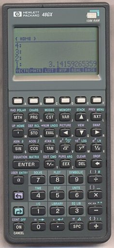
HP reached the same conclusion in 1984 with the Saturn processor, used in the HP-71B and later the entire HP-28 and HP-48 series. Saturn registers are 64 bits wide (16 nibbles), operations work on user-selectable fields of those registers (one nibble, two nibbles, the whole register, and so on), and the instruction encoding is built entirely around nibble-granular access. The architecture powered HP’s high-end calculators for nearly twenty years. It is the most refined nibble-serial BCD processor ever built, and studying its instruction set before designing this one was instructive (both for what to copy and for what to deliberately do differently).
The Constraints That Drive Everything
Before drawing any instruction boxes, I listed what the CPU needed to be good at:
Nibble operations. The ALU should operate on 4-bit values natively. Addition, subtraction, comparison: all operating on nibbles, with BCD-adjust instructions (DAA and DAS) to keep results within decimal range after each step. The general-purpose registers are also nibble-wide (4 bits each), which is really narrow but feel like a natural fit to the rest of the architecture: a machine built around decimal digits should have registers the same size as a decimal digit.
Simple decode. I wanted the hardware decode logic to be simple and regular. Hence, the same class of operands should always occupy the same bitfields. If an instruction class needs an immediate operand, or a GP register index as a destination operand, it should always find it in fixed slots (like bits[3:0] or [7:4]). Instructions that share similar structures share the same decode rules. This also made the assembler much simpler to write.
Address Width Address space is finite, and I had to predict how much of it would I need. In this implementation, I closely tied it to the instruction widths, to be 12-bit wide.
Compact instructions. I settled on 12-bit fixed-length instructions. This is somewhat an unusual width, but it fits three nibbles exactly, which maps cleanly onto our nibble-oriented everything-else. An 8-bit instruction width was too limiting; 16-bit felt unnecessarily generous for this instruction set.
The 12-bit choice has a historical precedent worth noting: the PDP-8 minicomputer (1965) also used 12-bit instructions and a 12-bit address space of 4,096 words. Ken Olsen’s team at DEC arrived at 12 bits for similar reasons: enough opcode space, enough address reach, nothing wasted. The PDP-8 went on to sell tens of thousands of units and influence a generation of computer architects. The parallel is coincidental.
Harvard memory model. Instruction and data address spaces are completely seperate. This was a deliberate choice to maximize the room each can grow into independently: code can expand to a full 4,096 twelve-bit instruction words without competing with data space, and the data bus is a narrow 4-bit nibble-wide path tuned to the data width rather than to instruction fetches.
Register-rich. Since the instruction encoding is partitioned into nibble-wide (4-bit) fields, register indices naturally fit into 4 bits, which yields 16 possible general-purpose registers (R0–R15). That felt like a lot, and I was not sure if 8 would be enough, but I knew that 16 registers might be an overdesign. Rather than commit either way, I made it a SystemVerilog parameter: the design supports either 8 or 16 GP-registers, and you pick at synthesis time, with only about a 3% difference in logic elements. I started writing microcode with 8 registers and kept a close eye on whether I would run out. I never did. Eight registers were sufficient throughout, so 16 were never enabled. The parameter is still there for anyone who wants it. The only drawback (or a price to pay) is that we are wasting one bit of instruction encoding with only 8 registers.
The result is a load-store architecture with Harvard memory (separate instruction and data buses), a 12-bit instruction ROM, and a 4-bit-wide data space, each addressable up to 4096 word locations.
The Instruction Set
Having a rough idea what I want to build, I started sketching the opcode map. Z80 (from years of hobbyist use) and ARM and x86 (in professional work) were the main influences on the instruction names, the flag conventions, and the general shape of the set. When you are both the architect and the only programmer, familiar patterns reduce errors. But the dual role cuts both ways. The freedom is extraordinary: no backward compatibility, no installed base to protect, no committee to approve a new opcode. If the ISA needs an instruction, you add it. If an instruction turns out to be useless, you remove it right away. Commercial CPU teams (the kind Tracy Kidder immortalized in The Soul of a New Machine, where hardware engineers and software engineers were distinct tribes who barely spoke) never have that fluidity. On the other hand, you carry a dangerous blind spot: you are the least qualified person to notice when an instruction is awkward, because you designed it and your mental model of the code naturally flows around its shape. The early HP calculator designers had the same problem. The teams who built the Woodstock series chips in the early 1970s were simultaneously defining the instruction set and writing all the microcode, and the HP Journal from that era documents exactly this: the November 1975 issue describes how several improvements to the Woodstock instruction set were driven by friction discovered deep in the microprogramming process (things that looked fine on paper but made the programmer’s life harder in practice). They fixed it by the next chip revision. I fixed things by the next commit.
Naturally, the instruction set wound up with roughly these groups:
- Load/store:
LDM,STM,LDI(load immediate),LDX/STX(indexed, for walking through register arrays), plus a two-register indexed variantLDX2/STX2for accessing 2D array of mantissas - ALU: 14 operations:
ADD,ADC,SUB,SBC,AND,OR,XOR,CMP,BIT(bit test),INC,DEC,DECA(decrement, selective flags),BCPL(9’s complement, for BCD negation), andBSHR(BCD shift right, divide by 2).DAAandDAS(BCD digit adjust) are separate instructions, not part of the ALU opcode group - Multiply:
MULmultiplies two nibbles (R0 × R1) and returns a 2-nibble result in {R1, R0}, using a lookup table in ROM rather than a hardware multiplier - Control flow:
JMP/JC/JNC,CALL/CALLC,RET/RETC,BRA/BRACfor short branches,HALT/HALTC - Register move and compare:
MOVfor inter-register copies,CMPXto compare any register against an immediate value - Flag manipulation:
SETF,CLRF,INVF(set, clear, invert any of the 16 flag bits by index),PUSHF/POPF,FLGET - I/O:
LCDWC(write control word to LCD),LCDWD(write ASCII string),LCDWR(write a register’s value as a hex digit) - Stack and address pointer:
PUSH/POPfor the data stack,ASTORE/ALOADfor sequential bulk register save/restore via the address pointer,APLDR/APSTRto load and save the address pointer itself
The complete instruction encoding table, including all opcode groups, condition flags, and ALU flag effects, is in the CPU ISA Reference in the repository’s docs/ folder. Here are just the main portions split into three tabs:
| Mnemonic | Opcode | Description |
|---|---|---|
| Misc & System | ||
| NOP | 0000 0000 0000 | No operation. Simulation apps use it to yield. |
| MUL | 0000 0000 0001 | BCD multiply {R1,R0} = R1 × R0 |
| DAS | 0000 0000 0010 | Decimal adjust R0 (after subtraction) if B flag is set |
| DAA | 0000 0000 0011 | Decimal adjust R0 (after addition) if B flag is set |
| POPF | 0000 0000 0100 | Pop ALU flags |
| PUSHF | 0000 0000 0101 | Push ALU flags |
| APLDR | 0000 0000 0110 | Load address pointer with {R2,R1,R0} |
| APSTR | 0000 0000 0111 | Store address pointer to {R2,R1,R0} |
| FLGET | 0000 0000 1000 | Read a condition flag indexed by R0 and set CF accordingly |
| 0000 0000 1001 | (unallocated) | |
| 0000 0000 101- | (unallocated) | |
| 0000 0000 11– | (unallocated) | |
| Flag Manipulation | ||
| INVF | 0000 0001 cccc | Invert selected flag bit (z, c, b, a; or <0,15>) |
| CLRF | 0000 0010 cccc | Clear selected flag bit |
| SETF | 0000 0011 cccc | Set selected flag bit |
| EI | 0000 0010 1111 | Enable interrupts — alias for CLRF 15 |
| DI | 0000 0011 1111 | Disable interrupts — alias for SETF 15 |
| Halt & I/O | ||
| HALTC | 0000 010n cccc | Conditional halt (n=0: if cond=1; n=1: if cond=0; or always when n=1, c=15) |
| HALTNC | 0000 0101 cccc | Alias for halt with negated condition |
| HALT | 0000 0101 1111 | Always halt |
| LCDWR | 0000 0110 rrrr | Write register as HEX digit to LCD module (polling LCD) |
| 0000 0111 —- | (unallocated) | |
| Return & Stack | ||
| RETC | 0000 100n cccc | Conditional return (n=0: if cond=1; n=1: if cond=0) |
| RETNC | 0000 1001 cccc | Return with negated condition |
| RET | 0000 1001 1111 | Unconditional return |
| RETI | 0000 1000 1111 | Return from interrupt; clears FLAG_IRQ_DIS |
| POP | 0000 1100 qqqq | Pop R0–Rq; increment stack pointer |
| PUSH | 0000 1101 qqqq | Push R0–Rq; decrement stack pointer |
| ALOAD | 0000 1110 qqqq | Load R0–Rq from data memory; increment address pointer |
| ASTORE | 0000 1111 qqqq | Store R0–Rq to data memory; increment address pointer |
| ALU — Register Operands | ||
| CMP | 0001 0000 rrrr | Compare reg with R0; sets CF if R0<reg, ZF if equal. Non-committing. |
| ADD | 0001 0001 rrrr | R0 = R0 + reg |
| ADC | 0001 0010 rrrr | R0 = R0 + reg + carry |
| SUB | 0001 0011 rrrr | R0 = R0 – reg |
| SBC | 0001 0100 rrrr | R0 = R0 – reg – carry |
| AND | 0001 0101 rrrr | R0 = R0 & reg |
| OR | 0001 0110 rrrr | R0 = R0 | reg |
| XOR | 0001 0111 rrrr | R0 = R0 ^ reg |
| 0001 1000 —- | (unallocated ALU — non-committing) | |
| INC | 0001 1001 rrrr | Increment any register |
| DEC | 0001 1010 rrrr | Decrement any register |
| DECA | 0001 1011 rrrr | Decrement; sets AF and ZF only |
| BCPL | 0001 1100 rrrr | BCD complement: CF, reg = 9 – reg + CF |
| BSHR | 0001 1101 rrrr | BCD-adjusted shift right: reg = reg/2 + (CF ? 5 : 0) |
| 0001 111- —- | (unallocated ALU) | |
| ALU — Immediate Operands | ||
| CMPI | 0010 0000 iiii | Compare R0 with immediate; R0 unchanged. Non-committing. |
| ADDI | 0010 0001 iiii | R0 = R0 + immediate |
| ADCI | 0010 0010 iiii | R0 = R0 + immediate + carry |
| SUBI | 0010 0011 iiii | R0 = R0 – immediate |
| SBCI | 0010 0100 iiii | R0 = R0 – immediate – carry |
| ANDI | 0010 0101 iiii | R0 = R0 & immediate |
| ORI | 0010 0110 iiii | R0 = R0 | immediate |
| XORI | 0010 0111 iiii | R0 = R0 ^ immediate |
| BIT | 0010 1000 00tt | Test bit tt of R0; sets CF if bit=1. Non-committing. |
| 0010 1001–111- —- | (unusable aliases / unallocated ALU) | |
| Load, Move & LCD | ||
| LDI | 0011 iiii rrrr | Load immediate value to a register |
| LCDWC | 0100 iiii rrrr | Write 8-bit control word to LCD (top 4 bits = instruction, low 4 bits = register) |
| LCDWD | 0101 iiii iiii | Write 8-bit ASCII data to LCD |
| MOV | 0110 pppp rrrr | Move register p → register r |
| CMPX | 0111 rrrr iiii | Compare any register with immediate; CF set if reg<imm |
| Branch (PC-relative) | ||
| BRAC | 10nc csss ssss | Conditional relative branch (±64/63 displacement) |
| BRA | 1011 1sss ssss | Unconditional relative branch |
| Jump & Call (2-word, address follows) | ||
| JC | 1100 000n cccc | Conditional jump (n=0: if cond=1; n=1: if cond=0) |
| JNC | 1100 0001 cccc | Jump with negated condition |
| JMP | 1100 0001 1111 | Unconditional jump |
| 1100 001-–1— —- | (unallocated) | |
| KEYCALL | 1101 0000 0000 | Call key handler indexed by CPU key_code; dispatch table address follows |
| TBLCALL | 1101 0000 0001 | Call handler indexed by R0; dispatch table address follows |
| 1101 0000 001-–1— | (unallocated) | |
| CALLC | 1101 001n cccc | Conditional call (n=0: if cond=1; n=1: if cond=0); address follows |
| CALLNC | 1101 0011 cccc | Call with negated condition |
| CALL | 1101 0011 1111 | Unconditional call |
| 1101 01–1— —- | (unallocated) | |
| Memory Access (2-word) | ||
| LDM | 1110 0000 rrrr | Load register from memory; address follows |
| STM | 1110 0001 rrrr | Store register to memory; address follows |
| LDX | 1110 0010 rrrr | Load from base address + indexed offset; word 2: base(11:4) | index-reg(3:0) |
| STX | 1110 0011 rrrr | Store to base address + indexed offset |
| LDX2 | 1110 0100 rrrr | Load from base + two index registers; word 2: base(11:8) | idx2(7:4) | idx1(3:0) |
| STX2 | 1110 0101 rrrr | Store to base + two index registers |
| 1110 011- —- | (reserved — decoder pattern in Verilog) | |
| LDAP | 1110 1000 0000 | Load address pointer with immediate; address follows |
| 1110 1000 0001–11 … | (unallocated) | |
| CALLI | 1111 qqqq rrrr | Load r4=qqqq, r3=rrrr as arguments, then call subroutine; address follows |
15 condition bits. A condition code is a 4-bit selector into a single flag. Bits 3 and 15 can only be tested positively — negative variants encode unconditional instructions.
| Bit | Flag Name | Description |
|---|---|---|
| 0 | FLAG_Z | ALU: Zero flag |
| 1 | FLAG_C | ALU: Carry flag |
| 2 | FLAG_B | ALU: BCD flag — set on ADC/SBC when sum > 9, or on BCD borrow |
| 3 | FLAG_A | ALU: Set by DECA to signal a positive value is available. Only positive checks supported (brac a); negative variant encodes unconditional forms. |
| 4 | FLAG_S0_ZERO | Scratch register 0 value is zero |
| 5 | FLAG_S1_ZERO | Scratch register 1 value is zero |
| 6 | FLAG_IS_SUB | Operation is a subtraction, not addition |
| 7 | FLAG_OF | Sticky overflow bit |
| 8 | FLAG_DEG | Angles are in degrees (not radians) |
| 9 | FLAG_HYP | Using hyperbolic functions (not trigonometric) |
| 10 | FLAG_LIFT | Stack lift enable: 1 = lift on next digit entry; 0 = no lift |
| 11 | FLAG_TEST | Contains a Boolean result after a test operation |
| 12 | FLAG_EDIT_EXP | Input mode: 0 = editing mantissa; 1 = editing exponent |
| 13 | FLAG_INPUT | Input state: 0 = RESULT; 1 = INPUT |
| 14 | FLAG_AUX | Internal: skip display update; track decimal point printing |
| 15 | FLAG_IRQ_DIS | Interrupt disable (set on reset). Only positive checks supported (jc 15); negative variant encodes unconditional forms. |
14 ALU operations. X = first operand, Y = second, C = incoming carry, R = result. “R > 15” / “R < 0” means the nibble result overflowed (wraps to 0) or underflowed (wraps to 15). Operations marked (*) are non-committing — they update flags only, not registers.
| Operation | AF | BF | CF | ZF |
|---|---|---|---|---|
| CMP (*) | — | — | X < Y | X == Y |
| ADD | — | R > 9 | R > 15 | R == 0 |
| ADC | — | R > 9 | R > 15 | R == 0 |
| SUB | — | |R| > 9 | R < 0 | R == 0 |
| SBC | — | |R| > 9 | R < 0 | R == 0 |
| AND | — | — | — | R == 0 |
| OR | — | — | — | R == 0 |
| XOR | — | — | — | R == 0 |
| BIT (*) | — | — | R[n] == 0 | — |
| INC | — | R > 9 | R > 15 | R == 0 |
| DEC | — | |R| > 9 | R < 0 | R == 0 |
| DECA | R < 0 | — | — | R == 0 |
| BCPL | — | R > 9 | — | R == 0 |
| BSHR | — | R > 9 | X[0] | R == 0 |
| FLGET (*) | — | — | flag[R0] | — |
The ROM table approach for single-digit multiplication is simple and efficient. The original HP-35 (1972) had no hardware multiplier and no lookup table: it computed BCD multiplication through iterative shift-and-add in microcode, which kept the chip count to five custom ICs (two processor chips plus three ROMs) but was slow. The HP-35 team, working under Bill Hewlett’s directive to fit in a shirt pocket, made every transistor count.
One instruction added late in the process turned out to matter more than expected: CALLI (a call with an implicit argument passing convention). After the complete microcode was already written, I did an analysis of instruction frequency (2,604 instructions in the production microcode, not counting tests) and found that ldi and call together accounted for 28% of all code. I did not expect such a high number. The pattern was consistent: almost every call was immediately preceded by ldi instructions to load R4 and R3 with arguments. Once you start seeing it, it become obvious. Adding this instruction reduced the total code size from 3,451 words (84% of the 4,096 available) to 3,265 words (79%), a saving of 186 words or 5.3%. I find that kind of discovery genuinely satisfying: it is the ISA equivalent of finding a $20 bill in a back pocket.

The only reason I could even spot this (and some other) chance for optimization is because I wrote microcode while rigorously following identical patterns: always using the same set of registers to pass arguments to subroutines, the same patterns where a code sequence repeat was in place etc., basically, writing very “boring”, structured code, without trying to be too clever – perhaps a reason things mostly worked at the first pass.
John Cocke at IBM Research showed in the mid-1970s that roughly 20% of the instructions in a typical program accounted for about 80% of the execution. His finding was one of the foundations of the RISC movement: if only a handful of instructions dominate execution, optimize those and simplify everything else. David Patterson at Berkeley later coined the term RISC and published the Berkeley RISC-I processor in 1982, which had just 31 instructions in 44,000 transistors and demonstrated competitive performance with VAX-class machines on key benchmarks. The lesson was the same as the one in the CALLI optimization: measure what actually runs, then fix that.
My 2025 revision added several more instructions born from the same pattern-spotting process. TBLCALL handles scripting function dispatch: given a base address (second word) and an index in R0, it computes the jump target as base + R0 and then, mid-pipeline, transforms itself into an unconditional JMP (a neat trick that avoids an extra fetch cycle). DECA is a targeted ALU operation that decrements a register and updates only ZF and AF, leaving CF and BF untouched for chaining inner arithmetic operations. The AF flag is set if the pre-decrement value was nonzero and cleared if it was zero, which makes DECA the right tool for loop counters that need to test “was I already at zero?” rather than “did I just underflow?”
A few more changes related to adding the interrupts to the CPU are described in post 9.
One design detail worth calling out is how conditions are encoded. Every instruction that supports a condition has a 4-bit condition field in bits [3:0], selecting from 16 possible condition bits. The first four are the standard ALU flags (Z, C, B and A). The remaining twelve are general-purpose software flags, each settable, clearable and invertible by single-word instructions. Bit 4 of the condition field negates the selected condition, so the encoding for “if condition flag 1 is zero, do this” is 0b1_0001.
Conditional and unconditional instructions have identical encoding pattern – we detect a special case where condition flag number 15 with the negation bit set is treated as “always,” which elegantly avoids needing a separate unconditional instruction space.
The encoding works as follows:
| Condition | Encoding (n + flag) | Meaning |
|---|---|---|
JC z | 0 + 0000 = 00000 | Jump if zero flag is set |
JNC z (or JC nz) | 1 + 0000 = 10000 | Jump if zero flag is clear |
JC c | 0 + 0001 = 00001 | Jump if carry flag is set |
JC 7 | 0 + 0111 = 00111 | Jump if software flag 7 is set |
JNC 7 | 1 + 0111 = 10111 | Jump if software flag 7 is clear |
JMP (always) | 1 + 1111 = 11111 | Always (special value of all 1s) |
The assembler also accepts descriptive aliases: eq for zero set, ne for zero clear, lt for carry set, and ge for carry clear.
For branch instructions (BRA/BRAC), the condition field is only 3 bits wide (selecting from the four ALU flags only), with the special case {1,1,1} encoding the unconditional branch.
Jumps and calls need a full 12-bit target address, which arrives as a second instruction word. That works fine for long-range transfers, but it costs two words for every branch. For the short conditional branches that appear constantly in tight loops, spending two words is wasteful, but using only one word (12-bit) is not wide enough to add the address of the complete space. The BRA instruction is the compromise: a single 12-bit word encodes a 7-bit signed displacement (reaching -64 to +63 words in each direction) and a shortened condition set covering only the four CPU ALU flags plus the negation bit. That turned out to be sufficient for all inner-loop branching and also for many other short jumps if you structure your code wisely. The assembler also helps here: it detects when a jump target is close enough for BRA and suggests you to use the shorter form instead.
The ALU and BCD Arithmetic
The ALU is 4 bits wide and implements 14 operations. Most are straightforward; the interesting ones are the BCD support instructions.
After a nibble addition, the result might be between 10 and 15 (valid in hex, but not a legal BCD digit). The DAA instruction (Decimal Adjust after Addition) checks for this and adds 6 to bring the value back into the 0–9 range, also setting the carry flag for the next digit. DAS does the equivalent after subtraction, adding 10. Together these two instructions are what allow our nibble-serial BCD addition and subtraction algorithms to actually work in hardware. If DAA and DAS feel familiar, that is not a coincidence: they are lifted directly from an early 8086 processor, where they serve the same purpose.
The Z80 actually combined both adjustment cases into a single DAA instruction, reading the N flag (which the preceding subtraction sets) to decide whether to apply the addition or subtraction correction. The 8080 before it only handled the addition case. The 8086, by contrast, split them into two separate instructions (DAA and DAS) exactly as this design does. (Sometimes you accidentally agree with Intel.)
BSHR (BCD shift right) divides a digit by 2 and allows chaining (in microcode) across digits via the carry flag. It is a true decimal shift. The formula is x / 2 + (CF_in ? 5 : 0). When the previous digit is odd, its leftover half (5) passes down as carry-in and adds to the current digit. Carry-out is the digit’s LSB, passed to the next digit in the loop. The final carry out tells you whether the whole number had a remainder.
This instruction is functionally identical to the SRB (Shift Right BCD) micro-primitives found in the Hewlett-Packard Saturn architecture and the specialized BCD PLAs of the Texas Instruments TMS1100 and Hitachi HMCS40 series.
The Memory Map
The processor has two independent address spaces (Harvard architecture):
- Instruction space: 12-bit wide addresses, 12-bit wide instruction words (up to 4,096 instructions)
- Data space: 12-bit wide addresses, 4-bit wide data nibbles (up to 4,096 locations)
The calculator system data address space is laid out as follows:
Data Address Space
| Address_Range | Size | Region | Contents |
|---|---|---|---|
| RAM | |||
0x000–0x0FF | 256 | Register File | 16 registers × 16-nibble mantissa: X, Y, Z, T, LASTX, R (result), S0–S4 (scratch), 5 statistical accumulators |
0x100–0x11F | 32 | Exponents | 16 registers × 2-nibble exponent (high at 0x100, low at 0x110) |
0x120–0x12F | 16 | Sign Records | 16 registers × 1-nibble sign (bits: mantissa sign, exponent sign, validity) |
0x130–0x13F | 16 | System Variables | Display format, shift state, digit count, error code, guard digit, sticky bit, etc. |
0x140–0x209 | 202 | User Memory | STO/RCL registers 0–9 (mantissa, exponent, sign for each) |
0x20A–0x2FF | 246 | Free | Available for future use |
0x300–0x3FF | 256 | Data Stack | Grows downward from 0x3FF; guard at 0x300 triggers fault on underflow |
| ROM | |||
0x400–0x5FF | 512 | Constants ROM | Up to 32 full 16-nibble constants: π, e, ln(10), CORDIC/log tables |
| I/O | |||
0x600 | 1 | STRAPS / LED | Read: 4 hardware strap bits. Write: 4 front-panel LEDs |
0x601 | 1 | SYSCTL | System control (bit 0: printer enable) |
0x602 | 1 | PRNG | Read: random nibble from Galois LFSR |
0x603 | 1 | KEY_READY | Read: key-ready flag (bit 0). Write: clear key-ready |
| ROM | |||
0x800–0xFFF | 2,048 | Scripting ROM | Packed 4-bit tokens for the scripting interpreter |
0x000–0x3FF is RAM, holding everything the microcode works with directly. The first block (0x000–0x0FF) is the register file: the four RPN stack registers X, Y, Z and T each occupy 16 nibbles of mantissa, followed by LASTX, a scratch RESULT register, five scratch registers (S0–S4), and the five statistical accumulator registers (n, mean, running standard deviation, ΣX, ΣX²). Above those, all the exponents are stored separately in a compact block at 0x100: two nibbles per register, 16 registers side by side. Sign records follow at 0x120: one nibble each, with individual bits for mantissa sign, exponent sign, and a validity flag. System variables (display format, shift state, digit count, error code, and others) start at 0x130.
0x300–0x3FF is the data stack. The stack pointer initialises to the top of RAM and grows downward. The guard threshold SP_GUARD is set to 0x300: any push that would drive the stack pointer below that address triggers a CPU fault immediately, before the write happens. Too many pops wrap the pointer around to zero, which is also below the guard and also faults. In practice this caught several microcode bugs that would otherwise have taken more effort to localize.
0x400–0x5FF is the constants ROM: 512 nibbles of block memory, holding up to 32 full 16-nibble mantissas. This is where PI, e, and the CORDIC and logarithm lookup tables live. Accessing it and adds one cycle of read latency, matching the existing RAM timing.
0x600–0x7FF is MMIO. Writing to 0x600 controls the three LEDs; reading from it returns the four hardware strap bits (At the moment, I use straps to tell if display is attached for simulation). 0x601 is the SYSCTL register (bit 0 connects the printer to the LCD bus). 0x602 reads a fresh nibble from the Galois LFSR hardware PRNG. 0x603 reads the keypad state (key-ready flag) or clears key-ready on write. The key code itself is delivered to the CPU via a dedicated input port used by the KEYCALL instruction.
0x800–0xFFF is the scripting ROM: 2,048 nibbles of packed 4-bit tokens for the scripting interpreter.
The instruction space is entirely separate: a full 4,096 × 12-bit words of microcode ROM, with no competition from any of the above.
An Iterative Loop
A natural assumption is that you design the complete CPU first, then write the assembler, then write microcode. That is not how it went.
The actual process was a tight loop, one instruction at a time: add the instruction to the RTL, add its encoding rule to the assembler, assemble, write a test for it. Then run the test through Verilator (which compiles the Verilog into a cycle-accurate C++ model) and confirm that the instruction executes correctly and that it does not disturb anything it should not. Only once the test passed would I move on.
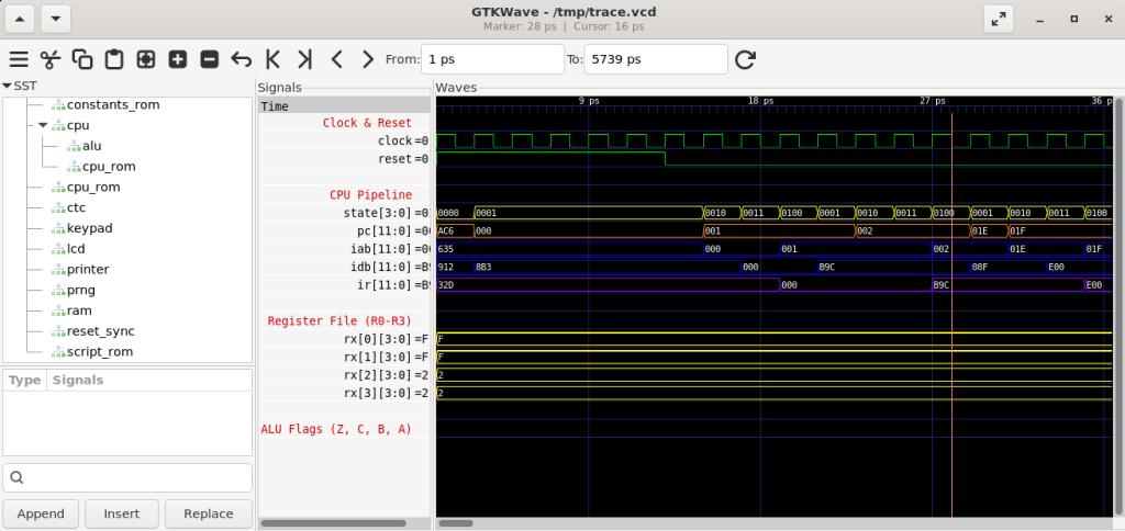
This was the only sane way to do it. Trying to build all the hardware first and test it all at once would have produced a debugging nightmare. The loop caught each problem early, before it became hard to isolate.
test_self_check.asm is the first level of defense. This test code runs every instruction, checks its result, and issues HALT if the result does not match specifications and/or expectations. HALT causes a fault in which it prints the faulting address, facilitating a quick check and also regression runs.
After getting a useful set of basic instructions working (which was a moving target), I would start writing microcode for one of the calculator functions. That is where I got a real feedback on the CPU design. Writing actual code quickly reveals whether the instruction set is right. You reach for something and it is not there. You find a pattern repeating everywhere and realize it should be one instruction instead of three. You discover that two instructions you thought were distinct could be generalized into one with an extra encoding bit, which both simplifies the decode logic and opens up new uses for it.
Sometimes I would remove an instruction entirely. There is a particular kind of temptation in CPU design: instructions that are elegant to think about but rarely needed in practice. They cost encoding space and decode complexity for almost no payoff. The discipline was to cut them. At one point I removed both BRANC and TEST after realizing the remaining conditional machinery covered their cases without the dedicated opcodes.
The internal calculator architecture was evolving in parallel throughout all of this: the locations of variables in memory, how registers are laid out, which scratch space is needed for what algorithm. Those decisions often fed back into the instruction design. The addressing modes for LDX2 and STX2, for example, only took their final form once the 16-nibble mantissa register layout was settled into a matrix that could be addressed simply with 4-bit indices laid out next to each other.
The assembler itself is a two-pass Python 3 script (casm.py), under 700 lines, supporting forward references, conditional assembly, multi-level file includes, local labels within procedures, expression evaluation and many other pseudo-directives (PROC, EQU, DEFINE) which deliberately echo MASM and TASM, partly because those tools shaped how I think about assembly, and partly because they established a good convention.
This iterative loop process felt less like engineering and more like sculpting. You start with a rough shape, and each pass reveals what needs to come off and what needs more work. The instruction set that emerged was not the one I would have designed on paper at the start. It was better than that.
The Strangest Thing About Designing Your Own ISA
There is something philosophically odd about writing code for a processor you designed. You know its internals completely: every state in the execution pipeline, every path in the decode logic. And yet, when you sit down to write microcode, you realize you do not know the processor at all. You do not know its personality. You do not know which sequence of instructions feel natural to use, which addressing modes are awkward in practice, which things you forgot or what edges start sticking out like thorns.
You also think differently about the code you write. With a standard CPU, you optimize for correctness and then performance. Here, you worry about something more fundamental: did I give myself the right tools? Every inefficiency in the microcode is a potential symptom of a missing instruction, or a wrong architecture. Every place where you reach for a workaround is a hint that the ISA may have a gap.
More microcode you write, you learn more, but also it is harder and more tedious to make changes. In the end, I am very happy with the instruction set and the overall CPU characteristics. It ended up perfect for this job.
The next post covers what happens when you actually try to write microcode for this ISA, and discover exactly which corners of the architecture you got slightly wrong.
If you have built your own CPU, or are thinking about it, I would love to hear about your experience. The design decisions you face are remarkably similar regardless of the target application, and comparing notes is always illuminating. Feel free to reach out or leave a comment.
The CPU and assembler source are in the FPGA-Calculator repository. The CPU specification document is in the docs folder.