This has been a long journey.
What We Built
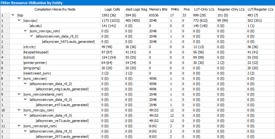
The earlier posts covered each layer in depth: the CPU, the arithmetic, the scripting interpreter, the hardware. Here is what the final Quartus synthesis report says about all of them together: The complete design uses 1,593 logic cells out of the 4,608 available on the EP2C5 (35% of the chip), with 594 dedicated logic registers and 17 M4K memory blocks. The CPU module itself accounts for 1,173 of those logic cells and 400 registers. The remaining logic goes to the peripherals: LCD driver (154 LCs), keypad scanner (97), thermal printer interface (64), CTC timer (49), and the hardware PRNG (20). The memory blocks break down as 12 M4Ks for the microcode ROM (49,152 bits: that is the entire calculator program), 2 for the scripting ROM (8,192 bits), 1 for the BCD constants ROM, 1 for the BCD multiplication lookup table inside the CPU, and 1 for RAM. I find that quietly satisfying: a working scientific calculator, all of it, in 35% of a small, cheap FPGA.
The Technology Stack
The project touched an unusual breadth of technologies: SystemVerilog for the CPU and peripherals, ModelSim and Verilator for simulation, Quartus for FPGA synthesis, Qt for the desktop simulator and WebAssembly browser demo, Python for the assembler and scripting compiler, C++ for the Proto reference implementation, and Autodesk Fusion for the enclosure. Each tool earned its place. What surprised me was how naturally they composed: the same Verilog source runs in every environment, the same test vectors verify both the C++ reference and the hardware, and the same Qt application compiles to desktop and browser without modification.
What I Learned
Designing your own CPU is surprisingly tractible. The EP2C5 has 4,608 logic elements. The CPU module uses 1,173 of them (the full design with all peripherals uses 1,593, or 35% of the chip). The learning curve is steep at first (Verilog is not forgiving of ambiguity), but once you have a testbench running and a waveform viewer open, debugging hardware feels more like software than most people expect. Verilator was the right tool: fast, free, and able to run the same RTL that ultimately goes into the FPGA.
BCD arithmetic is subtle in ways binary is not. The guard digit and sticky bit story took two rewrites of the prototype code to get right. The second rewrite happened because I found bugs in the first one while testing the microcode. That is exactly the reason you write a reference implementation before you write assembly. Having a golden reference that generates test vectors is not optional if you care about the last digit.
Writing your own CPU ISA is an adventure. You discover what your instruction set cannot express the moment you try to write real code in it. CALLI came from staring at an instruction frequency histogram and realizing that 28% of the code was just two-instruction preambles to function calls. The ISA you design on paper and the ISA you end up with after writing the software are rarely the same. And that is a good thing.
The scripting layer is the most elegant part of the design, in the engineering sense, it is delightfully compact. The Sinclair ZX Spectrum did the same thing in 1982. The insight is always the same: once you have a small set of primitives working correctly, a large fraction of the remaining functionality almost writes itself.
The physical build humbles you. Soldering a TQFP-144 at 0.5mm pitch is nerve-wracking the first time (I may have been slightly overconfident going in). Running a ribbon cable between two boards at a meetup is fragile and embarrasing. The jump from “works on the bench” to “works in an enclosure you can put in a bag” is larger than you expect, and most of the gap is mechanical, not electrical.
What Could Be Better
An honest accounting:
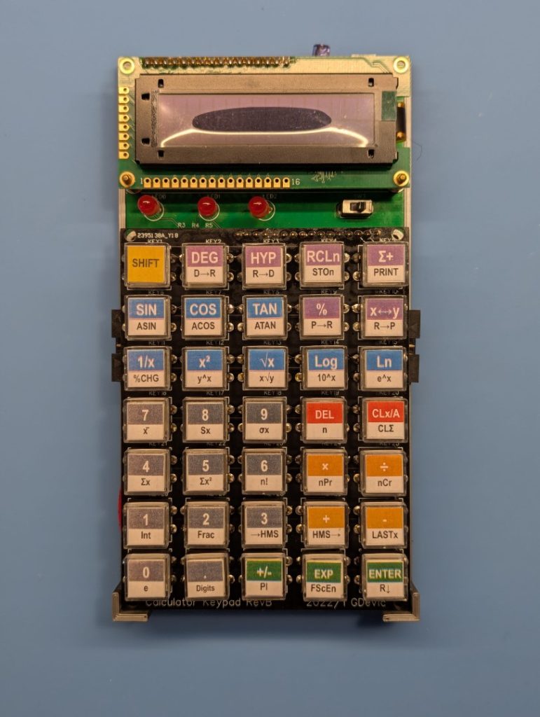
The keypad is the part of the project I am least satisfied with. Anyone who has used a vintage HP calculator knows how those keys feel: a firm, tactile click, zero wobble, legends that will never wear off because they go all the way through the plastic. Replicating that at home, even with a consumer 3D printer and a laser engraver, proved to be genuinely hard. I tried tactile and dome switches, push buttons and various prints over them, and a few other approaches. None of them bring full satisfaction yet, and I am still trying more things.
The CORDIC precision for large radian inputs is a known limitation. tanRad(1000) will not give you fifteen correct digits. Cody-Waite and Payne-Hanek both solve this, but at a code size cost I chose not to pay. However, a calculator that only accepts angles up to a few hundred radians before precision degrades is fine for most practical purposes.
I am still not 100% happy with how the calculator physically looks: it is too large, bulky and the keys, as mentioned, are imperfect. They are good for a hobby project, though.
Also, it really should be programmable. For that, it needs to have a storage that keeps the memory persistent. I am hoping to do another board spin with JLCPCB, so those could be the future improvements.
Closing Thoughts
The question I started with was: how does a scientific calculator actually work? I can answer it now, not in the abstract but in very specific terms. This project shows what BCD operations looks like at the digits level. It shows what CORDIC does to an angle and, overall, what takes to build a precise calculator.
The HP-35 microcode fit in 768 10-bit words. The complete design for this calculator uses 4k 12-bit words. In comparison, my design is massive! On the other hand, HP-41CX, the flagship calculator at the time, used 24k words, organized into pages.
The joy is in doing!
All source code is on GitHub. If you build something with any of it, or if you spot an error, I would like to hear from you.
Below is some raw footage I recorded while working on this project. I’m planning to put together a proper video for YouTube eventually (edited, narrated, the works), but that could take a while. Possibly a long while. In the meantime, these clips are unlisted and unpolished, but if you’re here, you probably don’t mind.
I hope you found something of value here.
This is an amazing project – congratulations!
Are you going to open source it?
I just did 🤗