Designing an FPGA Calculator from scratch
Try in Browser
This is a scientific BCD calculator that uses binary-coded decimals, the same internal number format HP used in its scientific calculators going back to the 1970s. It represents every decimal digit as a 4-bit nibble, which means perfect decimal accuracy, no floating-point conversion errors, and an architecture that is genuinely shaped by the problem it solves. To make that work cleanly, we also design a custom CPU that thinks in nibbles too. It runs on an Altera Cyclone II FPGA, synthesized with Quartus, simulated with Verilator and ModelSim, and debugged through a Qt-based desktop prototype that also compiles to WebAssembly if you want to run it in a browser. Several tools, several moving parts – all built in stages and tested at each one.
Across ten chapters, you will follow full arc: the architectural decisions and tradeoffs, the numerical algorithms (addition, multiplication, CORDIC for trig, logarithms), the custom CPU design and its 12-bit instruction set, a hand-written two-pass assembler in Python, the microcode that runs on that CPU, a scripting layer for high-level key functions, and finally the physical board with its battery, display, and keyboard. Each piece depends on the last, so we build them in order and test them before moving on because a calculator that returns wrong answers is considerably worse than a calculator that returns no answers at all.
The joy here is not in the finished device, though that does appear at the end. It is in each layer becoming real: the moment algorithms verified in C++ begin running on a processor you designed yourself, and the result is correct to 14 decimal digits. If you have ever wondered what actually happens inside that little machine when you press a key, this series is written for you. Hope you find something of value here.
Chapter 1 A Calculator (1): Introduction
The idea for this project came about during a week in February 2021 when the power grid failed here in Austin, Texas. The government’s handling of the situation was, sadly, memorable. With a gas fireplace as the only source of heat and light, and a weak phone data connection as the only link to the outside world, I had a few days to think about something new and exciting to do. I picked up my HP-41CV and started pressing its buttons. As always, it felt good. I suddenly wanted to create something like that myself!
Chapter 2 A Calculator (2): Pathfinding
Every serious project has a phase that nobody talks or writes about much. It comes before you have a design, before you have an architecture, before you are even sure any of it is possible. You pick a direction and walk until you hit a wall, then you turn and try another way. You build things just to understand them, then throw them away. Sometimes a tool you wrote in an afternoon ends up lasting for years. Sometimes a week of work goes straight into the trash. Sometimes you get happy with what you learned and never bother to complete your project. This is pathfinding, and it is not optional.
Chapter 3 A Calculator (3): Practical Numerical Methods

Post 2 answered the feasibility question: yes, tan, ln, exp, and sqrt can all be computed from add, subtract, and multiply alone, with some tricks. Post 3 is about doing it correctly, to up to 16 decimal digits, with a verified reference implementation that the hardware will eventually be tested against.
Chapter 4 A Calculator (4): The Framework
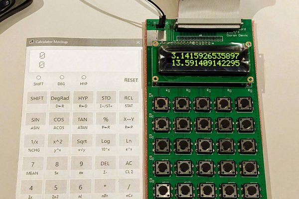
Before writing a single line of calculator code, there is a question worth asking: how do you test hardware that does not exist yet? In this installment, I describe the framework I set up to run a single Verilog source unmodified across four very different environments: ModelSim for signal-level simulation, Verilator for cycle-accurate C++ modeling, Qt for a desktop prototype with a debugger console, and WebAssembly so the same application runs in a browser without changing one line of RTL. The tools span both hardware and software developmentAll of the tools used here are free.
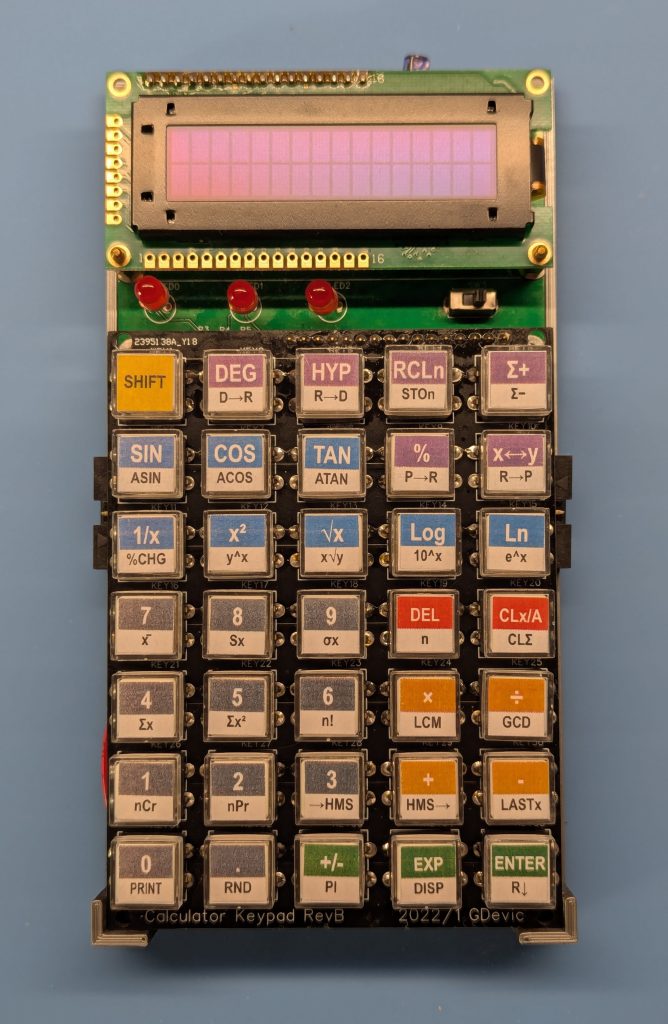
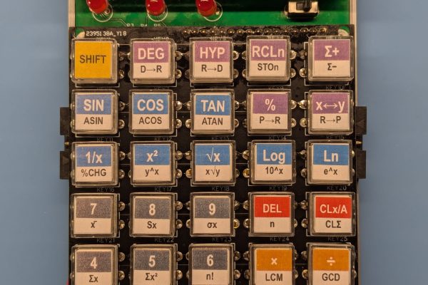
Chapter 5 A Calculator (5): The Hardware
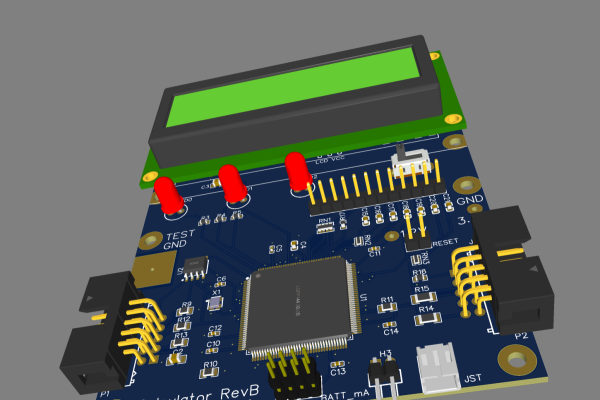
Everything up to this point lived in software. This post covers the first PCB order — a keypad matrix and OLED display board connected to the EP2C5 dev board by a ribbon cable — and what it takes to go from a schematic in a browser-based editor to a board you can actually type on. Simulation tells you the logic is correct; hardware tells you whether the timing works and the parts behave as the datasheet claims.
Chapter 6 A Calculator (6): Designing the CPU
No general-purpose CPU has nibble-addressable memory and addressing modes designed to walk a 16-digit BCD mantissa — so this post designs one. It covers the full instruction set architecture: 12-bit fixed-length instructions, a Harvard memory model, 14 ALU operations including BCD-adjust instructions borrowed from the 8086, and the iterative process of adding one instruction at a time, testing it in Verilator, and letting the microcode reveal what the ISA got wrong.
Chapter 7 A Calculator (7): Writing Microcode for a CPU You Just Invented
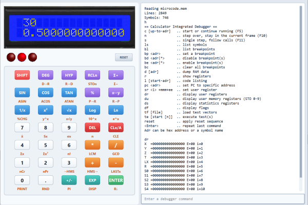
The C++ prototypes from earlier posts now pay off: each assembly file is a direct port of a verified reference implementation, tested against thousands of known-good vectors. This post covers writing the full calculator microcode — number input, display formatting, and the arithmetic functions — plus a small scripting interpreter that sits on top, letting complex operations like y^x collapse to six lines of tokens. Debugging it all runs through a Qt desktop simulator with source-level breakpoints, single-step, and live register inspection — because when something goes wrong in microcode, you cannot just add a print statement.
Chapter 8 A Calculator (8): From Dev Board to a Real Device
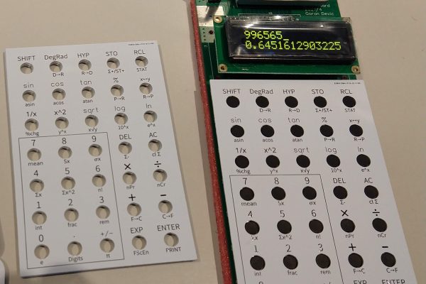
This post covers the hardware journey from a $5 EP2C5 dev board tethered to a ribbon cable to a single custom PCB with the FPGA soldered directly, a 3D-printed enclosure, and keycaps color-coded in HP's own yellow-and-red convention. Two programming connectors: JTAG for fast iteration during development, Active Serial for persistent flash, meant the edit-synthesize-test loop stayed quick right through to the finished device.
Chapter 9 A Calculator (9): Chasing the Last Digit
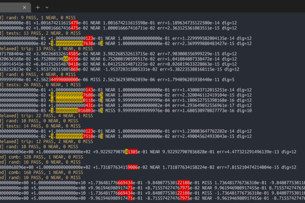
The 2021 implementation worked, but "most results correct to around 12 digits" is not the same as what a 16-digit BCD machine should deliver. This post covers the 2025 rewrite: a ground-up redo of the arithmetic engine with proper guard digit and sticky bit tracking, banker's rounding, a full trig suite, ten STO/RCL memory registers, and a hardware LFSR random number generator validated throughout against thousands of test vectors from a rewritten C++ reference. Interrupts were also added, mainly because the plumbing was interesting to design, and at 24 logic cells it would have been a shame not to.
Chapter 10 A Calculator (10): It Works!

The final post tallies everything: a working scientific calculator in 1,593 logic cells: 35% of a small, cheap FPGA with honest reflections on what the project taught and what it didn't quite nail. The keypad still isn't as satisfying as a vintage HP's, the TQFP-144 soldering was nerve-wracking, and the jump from "works on the bench" to "fits in a bag" was larger than expected. The joy, as always, was in the doing.
Nice project 🙂