In the previous post, I wrote about the microcode and the scripting layer. At that point, the calculator existed mainly in software: as a Qt desktop application running a verilated simulation, or as a WebAssembly page in a browser. That is a pleasant environment for development or for a showcase, but it is not a calculator. A calculator should sit on your desk. You should be able to pick it up and smack on the keys.
This post is about that step. Excluding smacking on the keys.
The Starting Point: An EP2C5 Dev Board
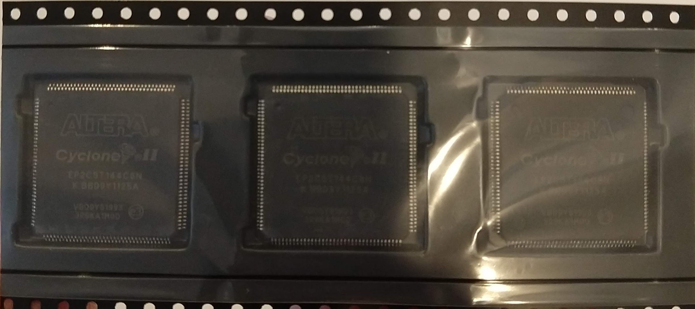
The first hardware to run the calculator code was not explicitly designed for it. It was a small, off-the-shelf, Altera EP2C5 Mini Dev Board (at that time available for around $5 on eBay), a credit-card-sized module that gives you a Cyclone II EP2C5T144C8 FPGA, a 50MHz oscillator, a few LEDs, a push button, and two 2×14 GPIO headers exposing most of the 144 FPGA pins. The lack of on-board peripherals is an advantage: nothing competes for GPIO pins, and there is no fixed resource usage to work around.
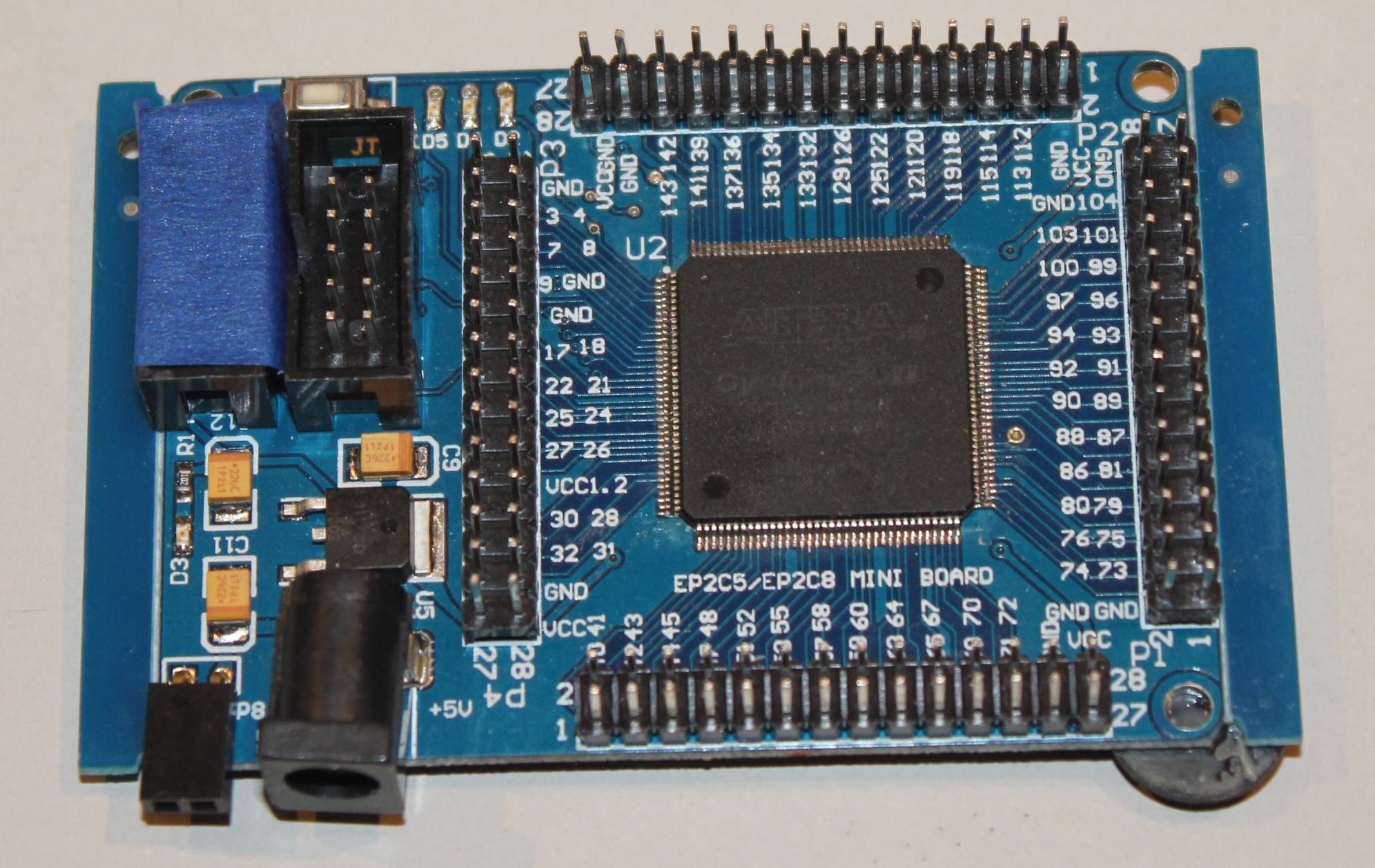
I have been using this board for several years just to play with FPGA. It is unpretentious and cheap. The FPGA itself is modest by modern standards (4,608 logic elements, 26 embedded multipliers, 89 user I/O pins), but it is more than sufficient for any project that I needed it for. The Cyclone II also requires Quartus 13.0 SP1, which is free and works fine for this device family.
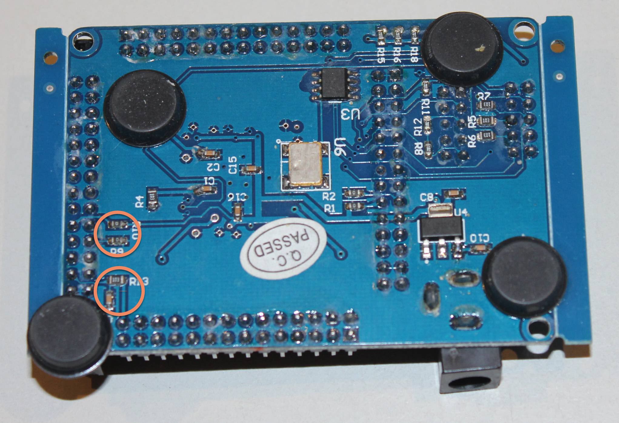
To use the board for the initial version of the calculator, I made a few small hardware modifications: I had to remove a couple of SMD resistors and capacitors that were routing GPIO pins to the wrong places for my pinout. Those components were only needed to support a different device SKU on the same board (the EP2C8), so removing them on the EP2C5 version was safe. The board’s website documents them clearly as “Only needed for EPC28.”
With those modifications done, the EP2C5 board became the CPU. To get a working calculator, I also needed a keypad and a display. Those lived on a separate PCB.
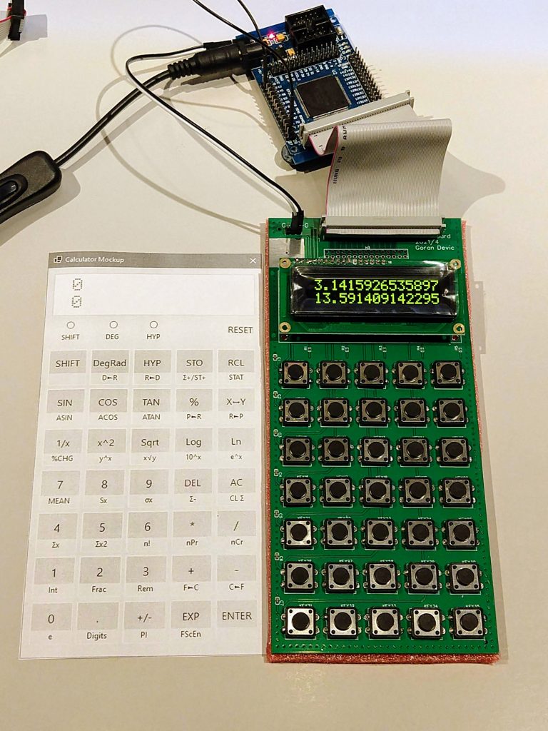
Rev A: Two Boards Connected by a Ribbon Cable
The Rev A configuration was the two-board setup described in Post 5: the EP2C5 module handling the FPGA, the custom PCB holding the display and 7×5 keypad matrix, connected by a 40-pin ribbon cable. The key matrix scanning, the HD44780-compatible OLED interface, and the EasyEDA/JLCPCB workflow are all covered there.
What Rev A Taught
Rev A worked.
My initial code was developed on it, and it worked. The calculator ran, displayed output, accepted key presses, and computed correctly. Having physical keys to press made a substantial difference to the development workflow: bugs that were invisible in the Qt simulator appeared immediately when a human finger was involved (timing edge cases in the keypad scanner, mostly). It also made it feel different: it was not “just” software running a Qt application – it was an actual hardware you can pick up and punch the keys!
But Rev A had obvious limitations: Two separate boards connected by a cable is not something you can easily (and safely!) carry around to meetups and show-and-tells. The cable was fragile and the assembly was finicky. There was no battery, no power switch, and no enclosure. It lived on a desk, tethered to a USB cable for power.
That was fine for development, but it was not fine for something you want to take out of a drawer and actually use.
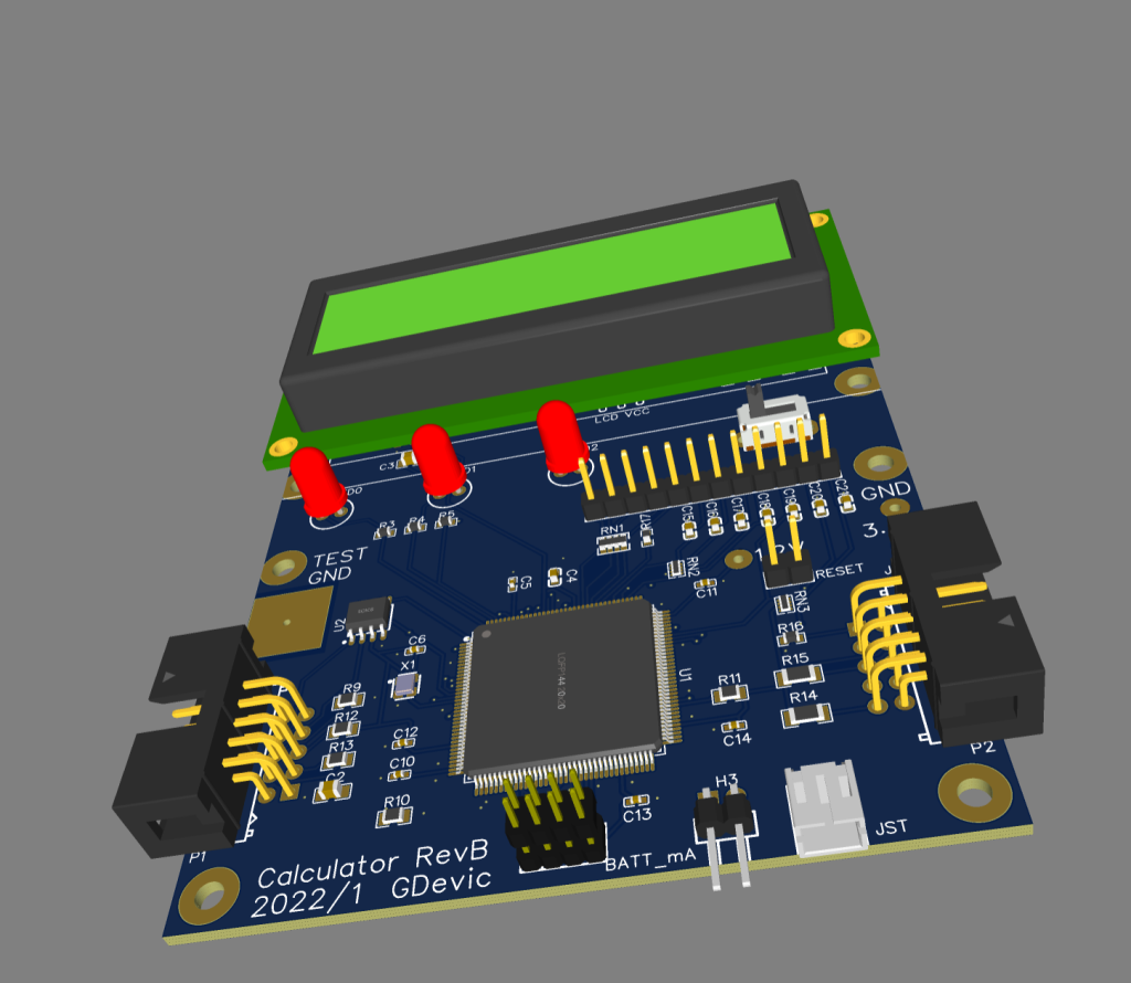
Rev B: One Custom Board
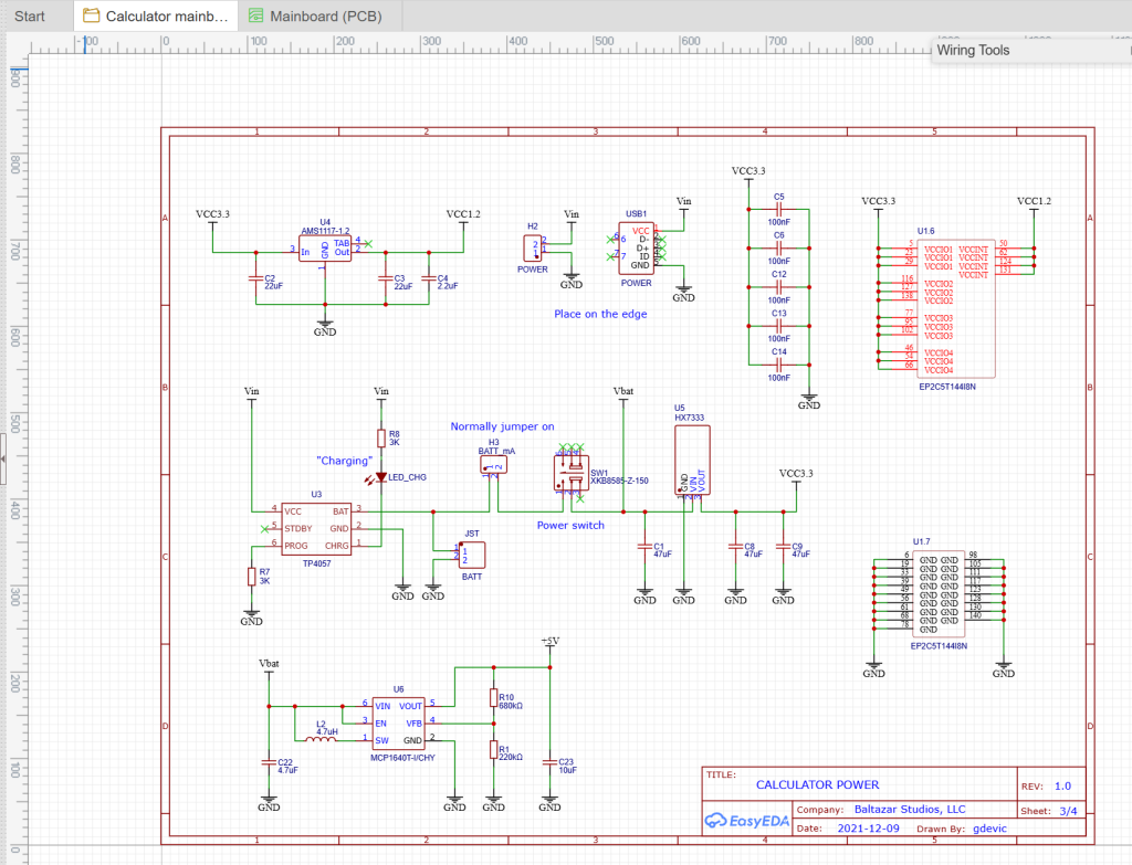
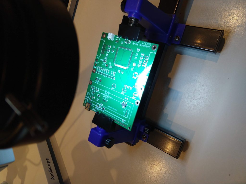
Rev B replaced the two-board arrangement with two custom PCBs. One integrated the bare EP2C5T144C8 FPGA chip (in TQFP-144 package), the display, the programming interfaces, and the power circuit. The second one was the keypad board. I had intentionally split the design into the main board and a separate keyboard: I had planned to play with several keyboard options, each using the same main board.
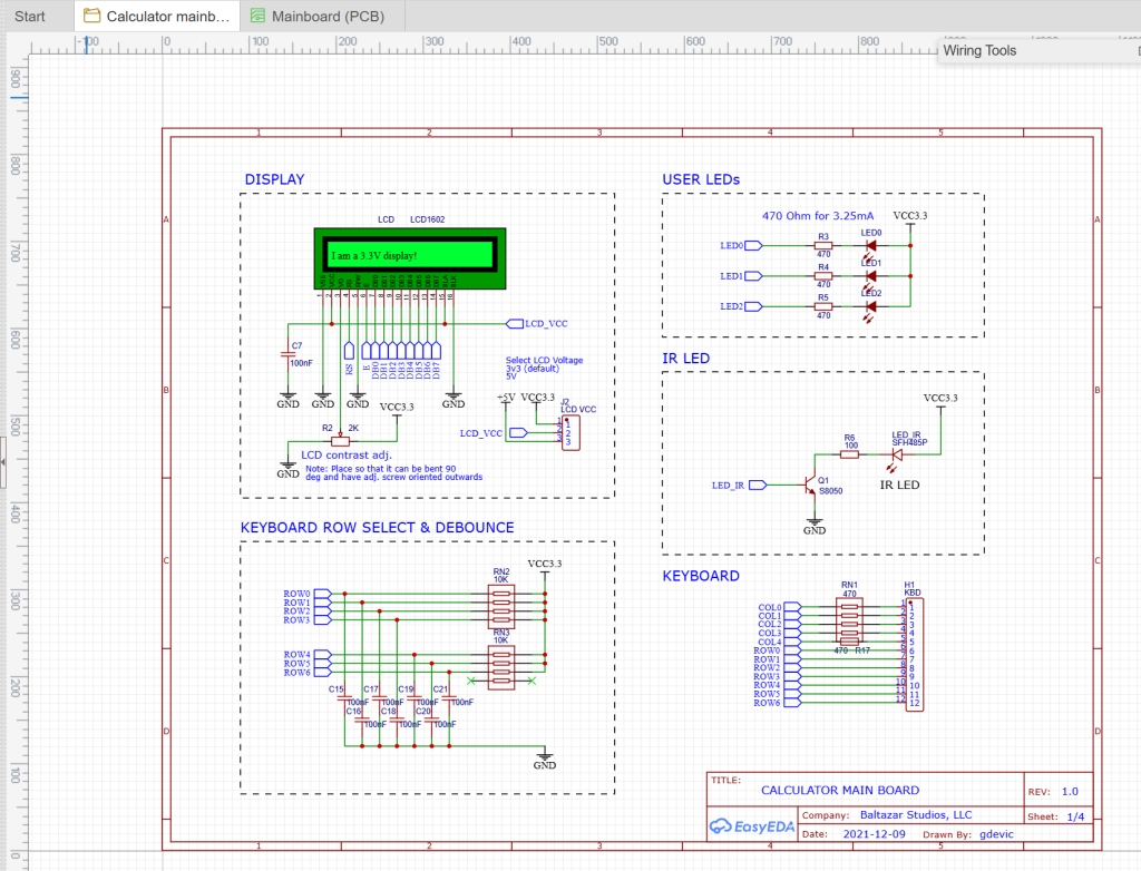
Keyboard, while maintaining the same 7×5 matrix of push-down keys, went through several layout revisions – and those were only software mappable revisions. For example, I kept modifying key function mappings as I re-evaluated which functions could be more useful, or better placed, on a different key.
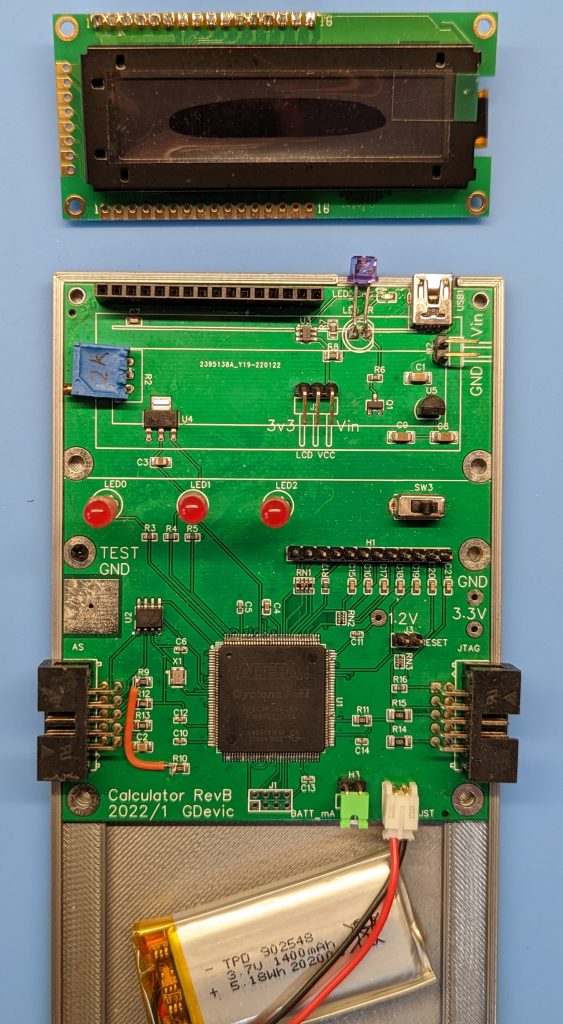
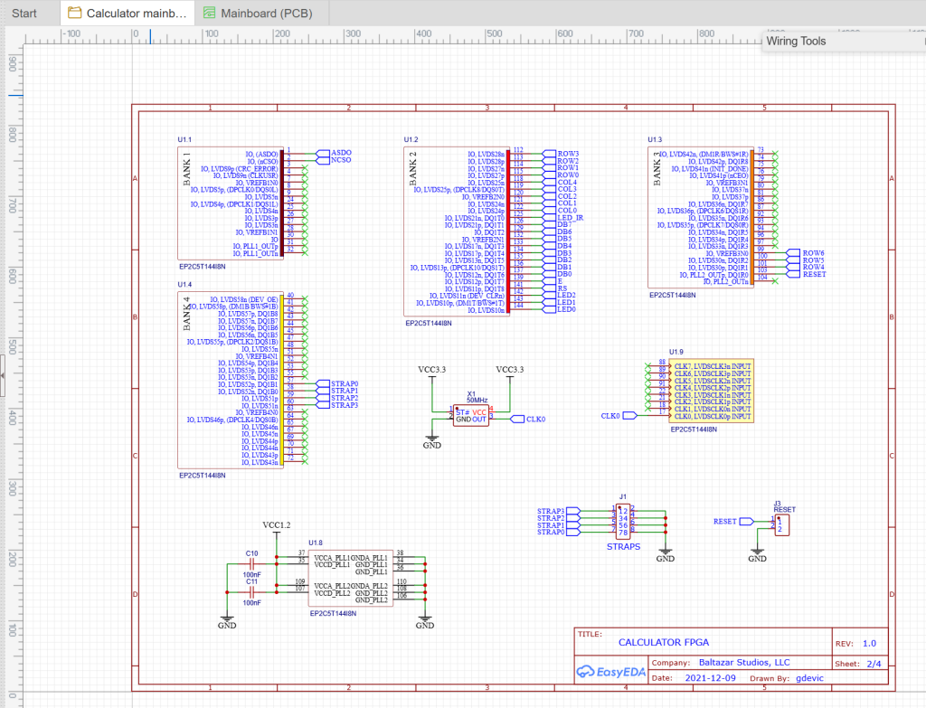
The FPGA
Although I am not that good at it, soldering a TQFP-144 package at home was manageable: with a decent iron, flux, solder wick, and patience. The pin pitch was 0.5mm. I used the drag-soldering technique: apply flux liberally, flow solder across the pins with the iron, then wick back the bridges. Under a 10x loupe, you check for bridges and cold joints. It takes about 30 minutes per chip and rarely needs more than two passes. I ended up with a few bridges, but those connect unused GPIOs and cause a horror only for people who solder well and who can also see tiny details.
The FPGA is the only truly complex component on the board. Everything else is through-hole or larger SMD.
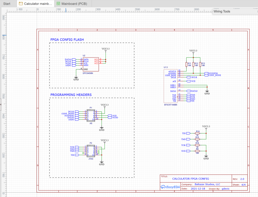
Two Programming Connectors
One of the design decisions that kept paying dividends was putting two separate programming connectors on the board, each wired to a different mode of flashing.
The right connector is wired for JTAG mode. Connecting a USB Blaster here programs the FPGA’s internal SRAM directly: the design is live instantly, but it vanishes on power-off. This is the mode used during development, because it is fast (a few seconds to program) and lets you iterate without wearing the flash memory.
It is worth noting what JTAG was originally designed for, because it was not this. The Joint Test Action Group formed in 1985 to solve a manufacturing problem: how to test board-level connections on increasingly fine-pitch packages without physical probes. Their solution, a standardized serial boundary-scan chain built into the silicon, became IEEE 1149.1 in 1990. Using JTAG to program and debug FPGAs came later, but the same four-wire access that lets you test pins is exactly what you need for programming, so the repurposing made sense.
The left connector is wired for Active Serial (AS) mode. Connecting the USB Blaster here programs the external EPCS flash chip, which holds the FPGA configuration across power cycles. When you power on the board, the FPGA reads its bitstream from the EPCS chip and configures itself in under a second. This is the “production” mode: program it once and the calculator starts up every time.
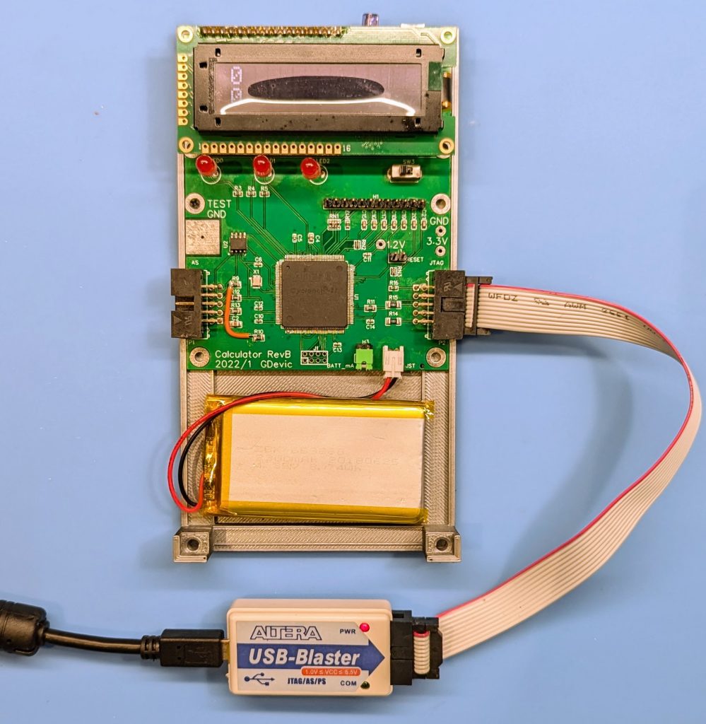
Both connectors use the standard 10-pin USB Blaster header. A single USB Blaster clone (around $10 on eBay) handles both, just plugged into the appropriate connector.
The Enclosure and Keycaps
The enclosure was designed in Autodesk Fusion and printed on a Prusa MK4S with PLA filament.

The yellow SHIFT key is a direct reference to HP’s own convention, and that convention has an interesting origin. The HP-35 of 1972 had no shift key at all: it only had an ARC key that toggled the trig functions between normal and inverse. When HP introduced the HP-45 in 1973, they added a yellow shift key that gave every key a second function and advertised it as “nearly doubling the computational power” of the calculator. That yellow key appeared on every HP scientific calculator for the next five decades. HP never changed it: anyone who has used one HP calculator knows what yellow means.
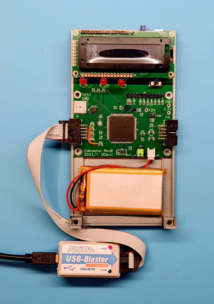
What It Looks Like to Program It
After synthesis in Quartus, programming the Rev B board takes about thirty seconds:
- Connect the USB-C cable.
- Plug the USB Blaster header into the left (AS) connector.
- Open the Programmer in Quartus, select Active Serial mode, add the
.poffile. - Click Start.
- Power-cycle the board.
The FPGA reads the bitstream from EPCS, configures itself, the OLED initializes, and the calculator is ready. From a blank screen to a working scientific calculator in a few seconds.
During development, steps 2 and 3 change: use the right (JTAG) connector, select JTAG mode, add the .sof file. The result is live in about three seconds and does not require a power cycle, which makes the edit-synthesize-test loop fast enough to be pleasant.
What Came from Rev A That Rev B Kept
It would be easy to treat Rev A as a throwaway prototype, but that would mischaracterize its role. Rev A was where the keypad scanner was written and debugged. The debounce timing, the scan frequency, the pull-up resistor values, the specific tactile switch model, the OLED initialization sequence: all of it was sorted out on Rev A before the custom board existed. Rev B benefited from a working, tested design for every peripheral.
The other thing Rev A established was the pin assignment discipline. The FPGA has 89 user I/O pins and the keypad scanner plus display interface uses about 22 of them. Choosing which physical pins map to which signals, and documenting that in the .qsf file, is the kind of decision that becomes very expensive to change once a board is manufactured. Getting it right on Rev A meant RevB‘s pin assignments could be carried over.
What Comes Next
The physical calculator now works, the microcode is complete. What the 2025 revision addressed was numerical precision: a rewrite of the core arithmetic algorithms based on the improved C++ prototype, tighter guard digit handling, and more CPU instruction optimization that reduced code size enough to add a few new functions. That is the subject of the next post.
Quartus project files (including RevA and RevB .qsf pin assignments) are in the quartus/ folder. The EP2C5 Mini Dev Board is documented at land-boards.com.