


Click on any image to open a higher-resolution version.
This is how it all works.
The sequencer is “the heart” of a CPU. It gets the external clock which in turn toggles two rows of flip-flops that generate machine cycles (M-cycles) and clock periods (T-states).
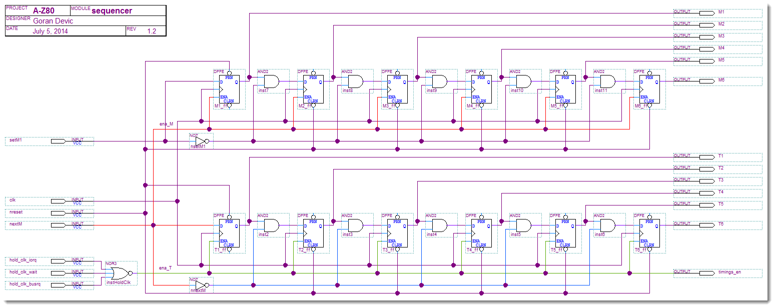
Simplified, if the sequencer would not have had any other input control signals, it would naturally want to activate M1+T1,T2,T3,T4,T5,T6; M2+T1,T2,T3,T4,T5,T6, and so on ad nauseam for as long as the input clock is coming in.
That sequence is, however, being manipulated by the execution engine at various times. For example, when an instruction is being completed, it signals “setM1” and the sequencer resets its counters back to M1/T1. Similarly, when a new functional sub-operation is needed (such as a read memory functional cycle), it issues “nextM” and the sequencer advances the M but resets the T count back to T1.
When servicing an interrupt, those timings get slightly modified: 2 clock periods are inserted to facilitate interrupt request propagation (signals “hold_clk1” and “hold_clk2”.) The following circuit inserts those two cycles:
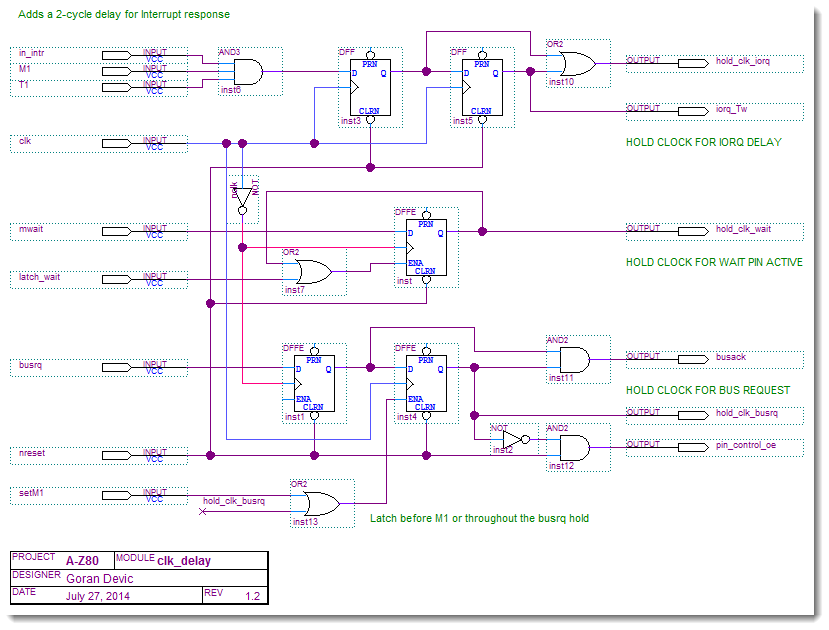
As you can see from the schematic, it happens – much like everything else – automatically, when the interrupt is being serviced (“in_intr” is active) and during the M1/T2 cycle.
How does the CPU load an instruction?
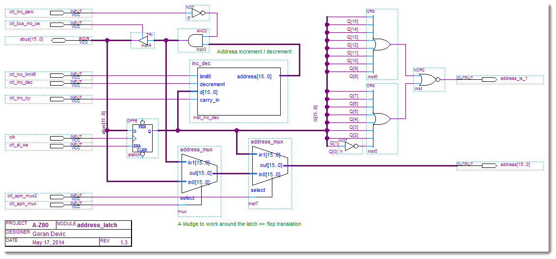
Address latch stores the current address as read from the PC (program counter) register and increments it to be ready for the next byte to load. Here is the address latch and the incrementing circuit:
The address is written into the address pins connected via the “address[15..0]”:
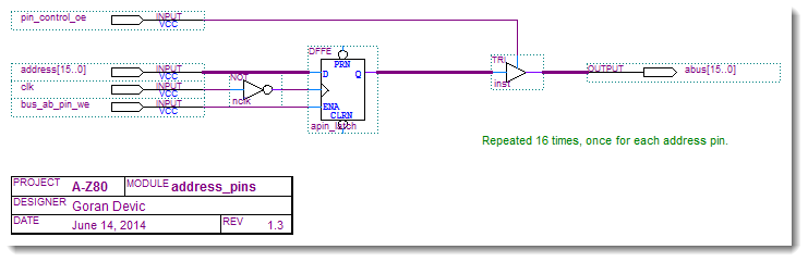
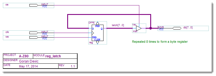
Each of the 16 address pins contains a latch that holds the address value on the external bus for the RAM/ROM to respond to. Once that happens, an instruction opcode is read into the CPU’s data pins:
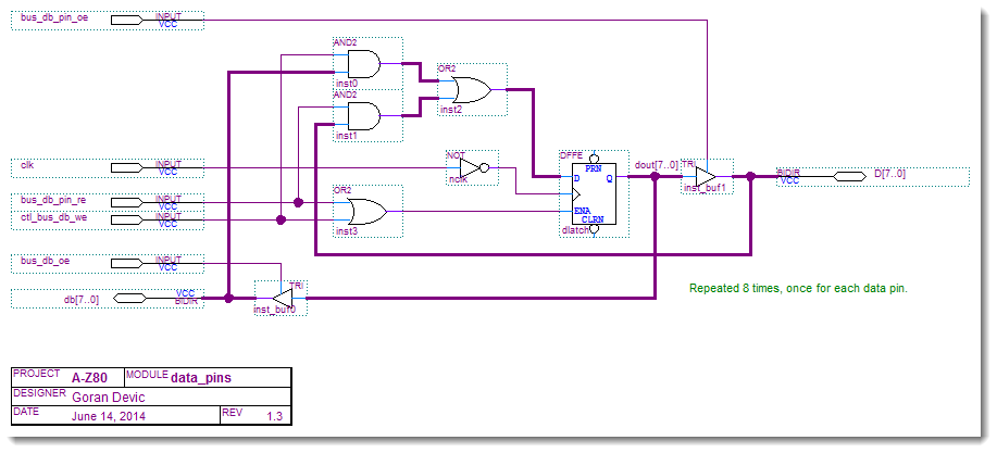
There are 8 data pins and they are a bit more complicated than address pins since they are bidirectional on both sides (on the external CPU and on the internal data bus side). Each data pin also contains a latch that stores the input value as well as holds a data value to be written out.
Through the internal data bus, the instruction opcode byte now gets stored into the IR (Instruction Register) which maintains its value until the next instruction is loaded.
It is very important that the IR holds the current instruction byte until a new instruction is ready to execute since the IR feeds into the PLA which is a matrix of gates that statically decode instructions. Z80 also overlaps instructions’ fetch/execute phases by 2 clocks, so each new instruction is loaded into IR at M1/T3 leaving the first 2 clocks to complete a previous instruction.
I already mentioned the address increment circuit that adds 1 to the address to prepare it to fetch a new byte. Here it is in a schematic:
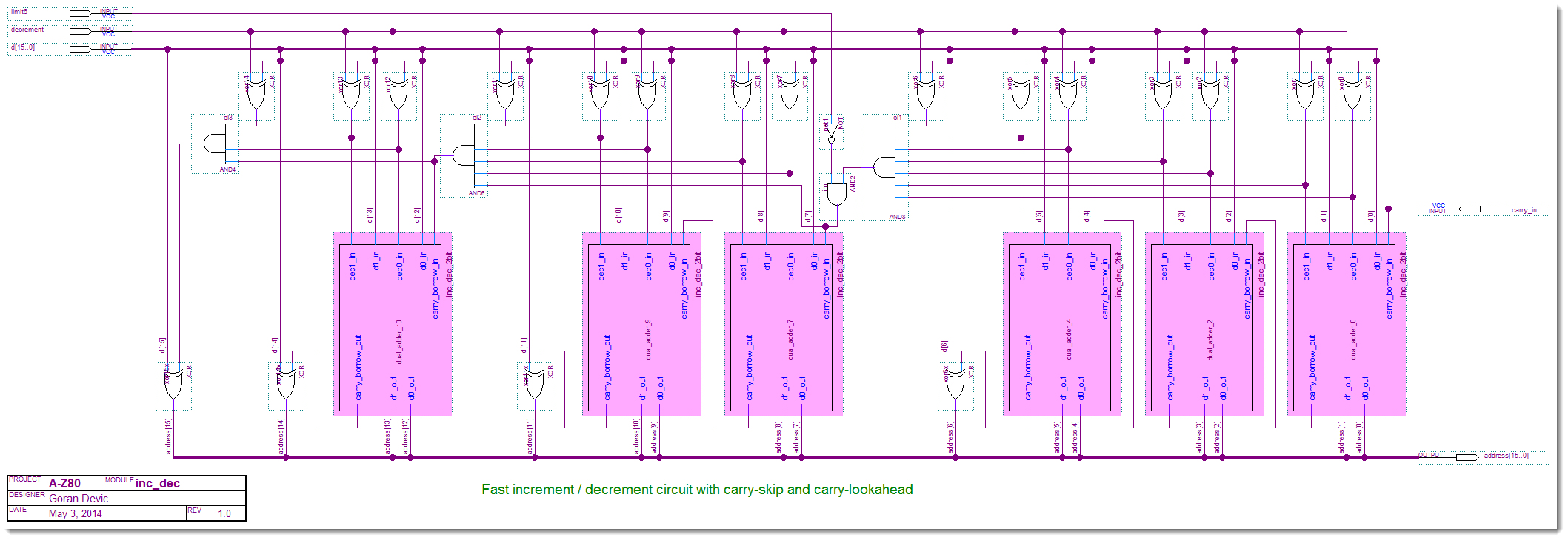
Ken described it well on his blog here. The core of the increment circuit looks like this:
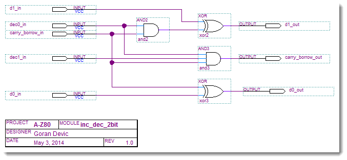
It is capable of incrementing and decrementing a 16-bit value, which in practice is mostly the address, but it could also be a register value during a 16-bit arithmetic operation.
The Register File contains all general purpose and system registers as latches. PC and IR are internally separated by a gate from the rest of the registers which allows the CPU to use them concurrently. For example, during the M1/T1 cycle PC is used to address the next opcode while at the same time a retiring instruction might be storing its final value into a general-purpose register.
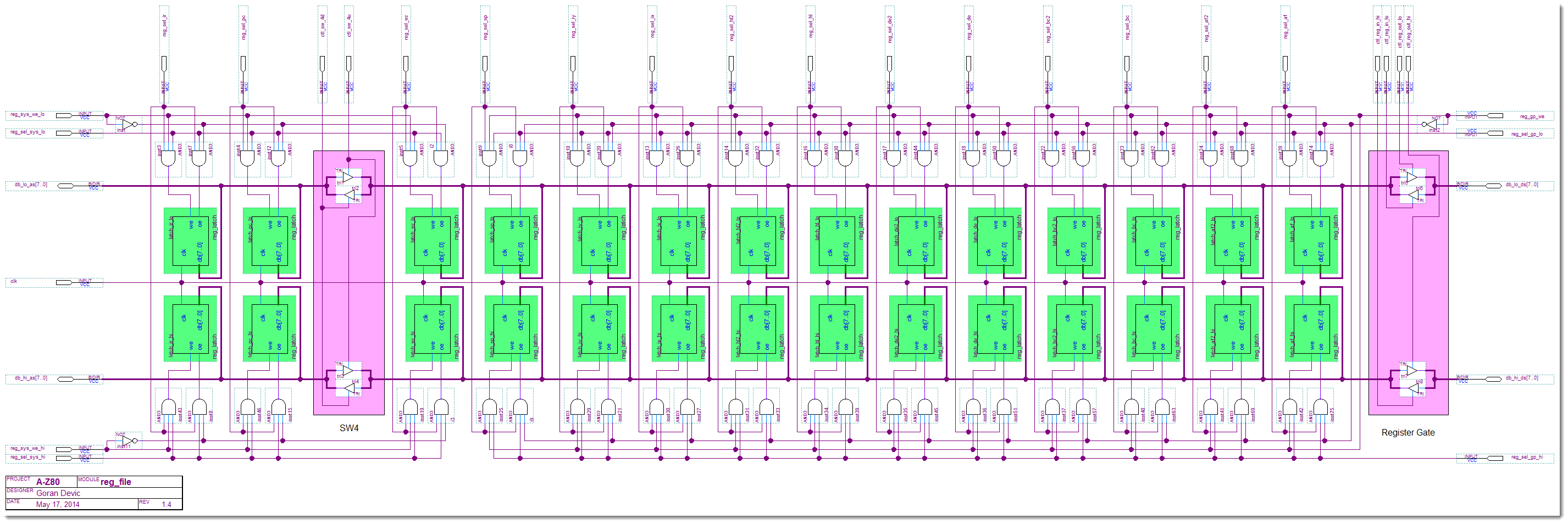
Each register in that sea of registers (talking in the spirit of 1976!) consists of an 8-bit data latch implemented as flip-flops in FPGA:
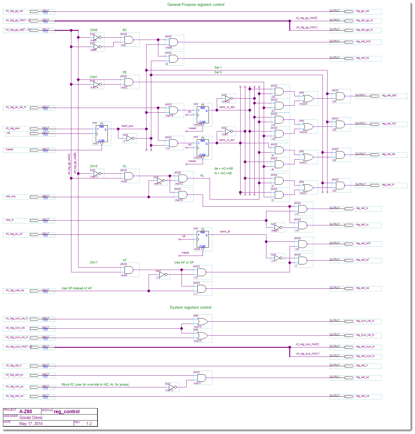
Z80 has 2 register banks and several ways to exchange registers – they are really not being exchanged but their control selection wires are through flops holding the state. In addition, different instruction groups index registers differently (for example, some instructions address SP instead of AF by the same bit combination). If that’s not enough, IX and IY registers are also sometimes used instead of the HL register.
This is the register control unit that takes care of all those combinations:
Here we touched on various, but not all, major blocks of the design. It is still not clear how it all works together, so read on…