This article contains a brief overview and a background of the A-Z80 CPU created for FPGA boards and a ZX Spectrum implementation tied to it.
(You can find the Russian translation of this article here: https://howtorecover.me/z80-s-nulya)
Every so often I let go of all that’s on my mind and simply brainstorm and play with new ideas and their combinations (mostly based on the retro stuff). Then I pick what seems to excite me the most and deep dive into it.
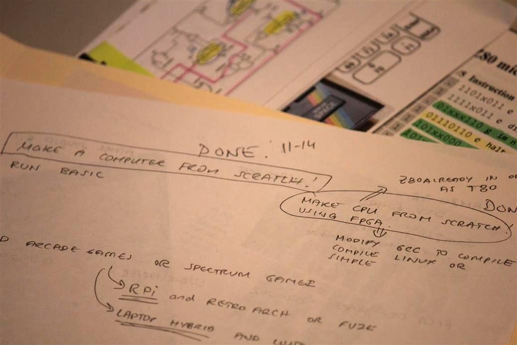
This time (early 2014), I wanted to re-make a Sinclair ZX Spectrum on an FPGA. There were already several implementations available and most of them used “off the shelf” components. One could simply pluck components written in Verilog (CPU, ULA) and with some glue logic quickly build a retro FPGA solution. There is no fun in doing that – or at least nothing much to learn about each component as one could learn by creating them from scratch.
I wanted to start with the Zilog Z80 CPU. Since real people design their own CPUs (right?!), I decided I would make my own version of it. 🙂
Both parts of this project (the A-Z80 CPU and a ZX Spectrum code that uses it) are fully described in separate blogs, and here I will try to tie them together using a somewhat less technical narrative.
I started reverse-engineering Zilog Z80 CPU about a year ago by running a working chip on a custom Arduino dongle board. I described it here. It was interesting to see how the pins responded to various scenarios. I was mostly interested in undocumented behaviour hoping it will give me some hints on the CPU’s internal architecture.
Then, I’ve found a set of articles by Ken Shirriff who actually reverse-engineered large portions of the Z80 from an image of a die. I’ve found the knowledge of “reading a die image” very exciting and the skill (in a weird way) very useful, so painstakingly I’ve learned to do the same. I reverse-engineered a few other pieces of that silicon, like the IR register and a data pin. Soon I got a hang of it and started “reading” other parts, as needed. It felt like a whole new world opened right in front of my eyes! Not much unlike stereogram images: as you look at it long enough, gates suddenly pop up in your mind and you start seeing transistors, pull-ups, and latches out of a tangled mesh of colorful flat traces.
I had purchased an Altera FPGA board with a desire to learn that technology after working on a project at my work which was using one, quite beefy, Altera chip. Designing circuitry on my own, I felt, was an exciting challenge and a great learning opportunity. Soon, I figured out how Verilog/SystemVerilog “works”; a language not too difficult to learn for any software person. I also brushed up on a logic design (I had one lousy taught EE class some 20 years ago).
Long story short, I started implementing selected parts of Z80 in the Quartus schematic editor and wrote related ModelSim tests one by one: first came the ALU (since its design was well described by Ken), then the register file, sequencer, etc. Frankly, I did not know how would all of that fit or work together; I was simply enjoying the process, one block at a time. I just loved seeing wires toggling and gates doing their thing in a ModelSim simulation: a certain deep understanding of a digital design sank in while playing with it.
I also read all I could get my hands on: patents on Z80 (and other CPUs) which provided valuable insights; talks, lectures, and over time I got a pretty good idea on how it all should work.
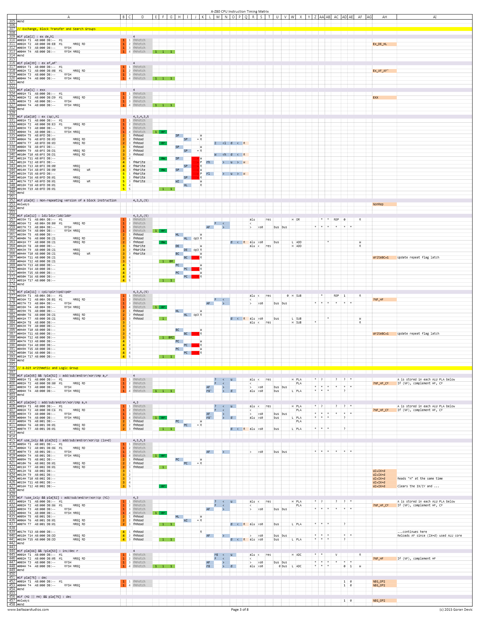
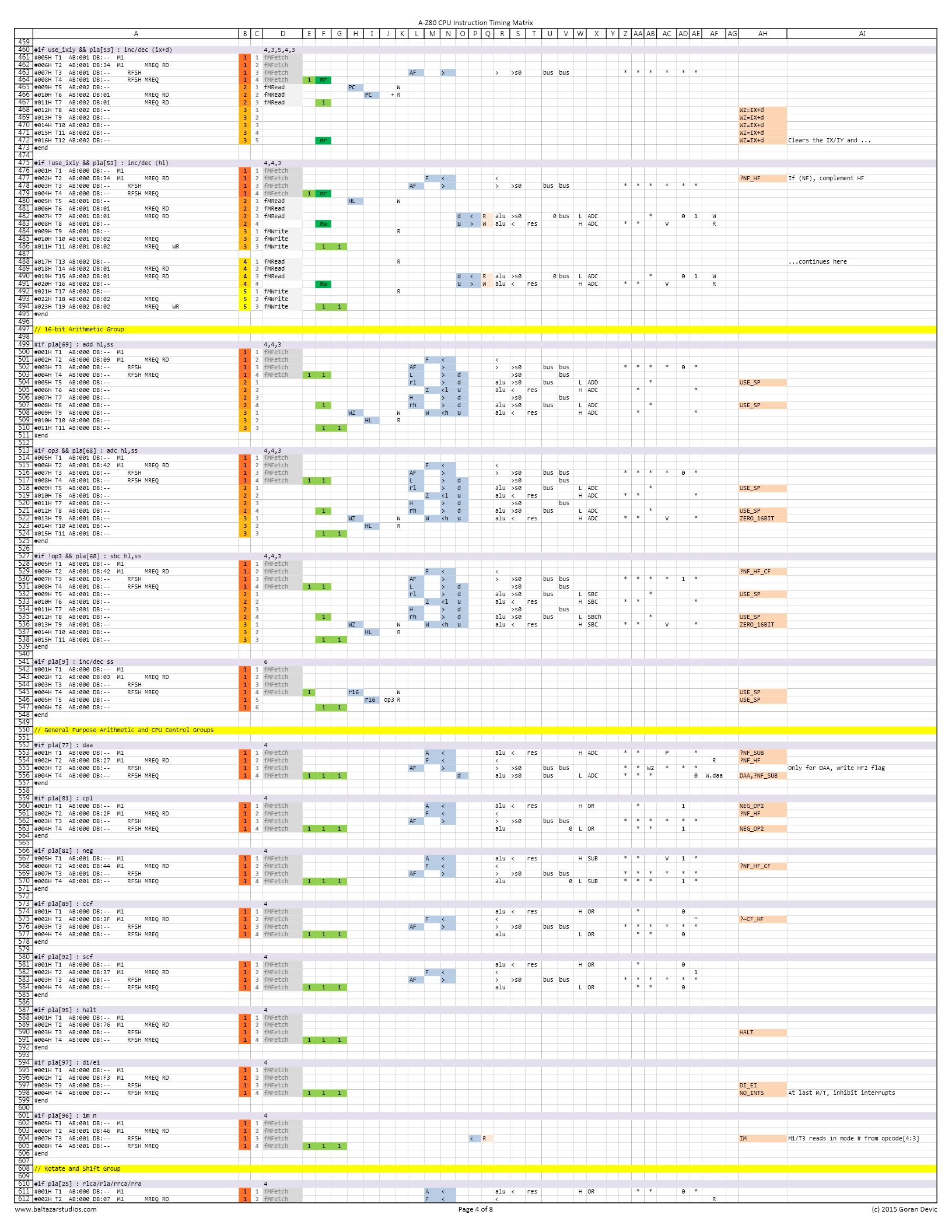
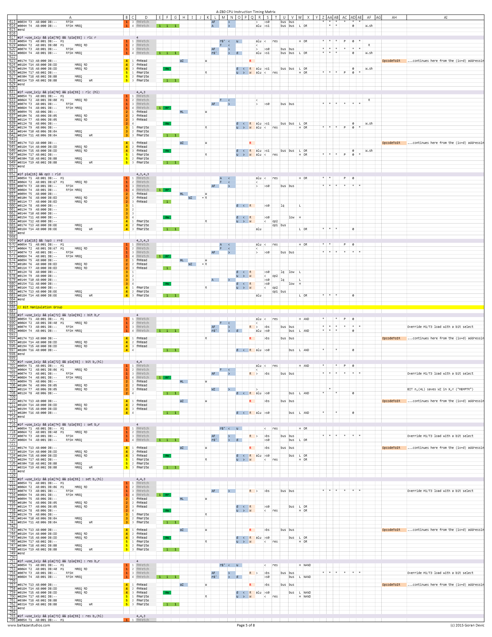
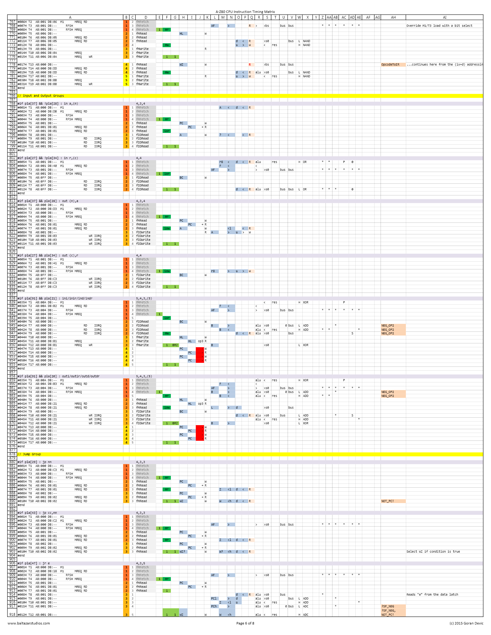
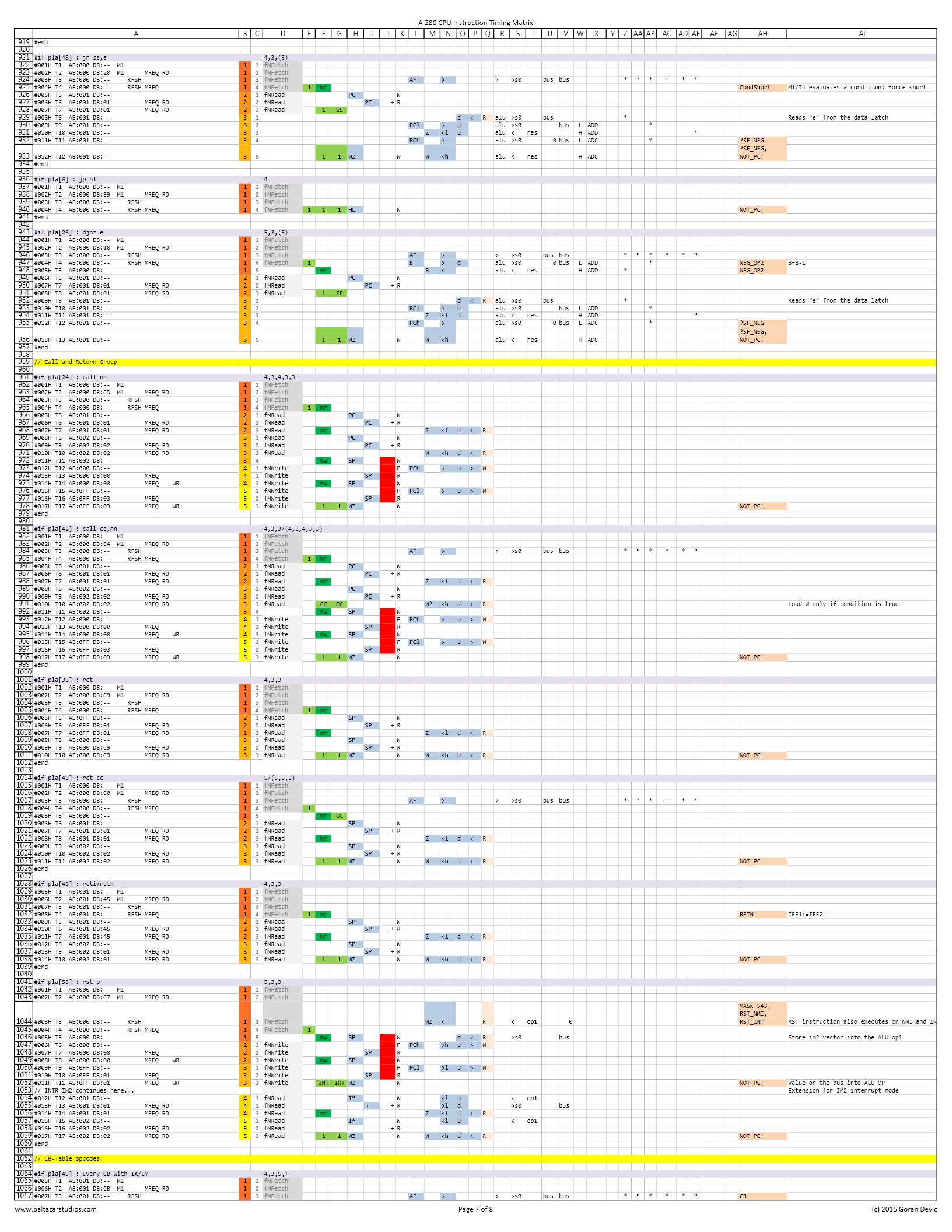
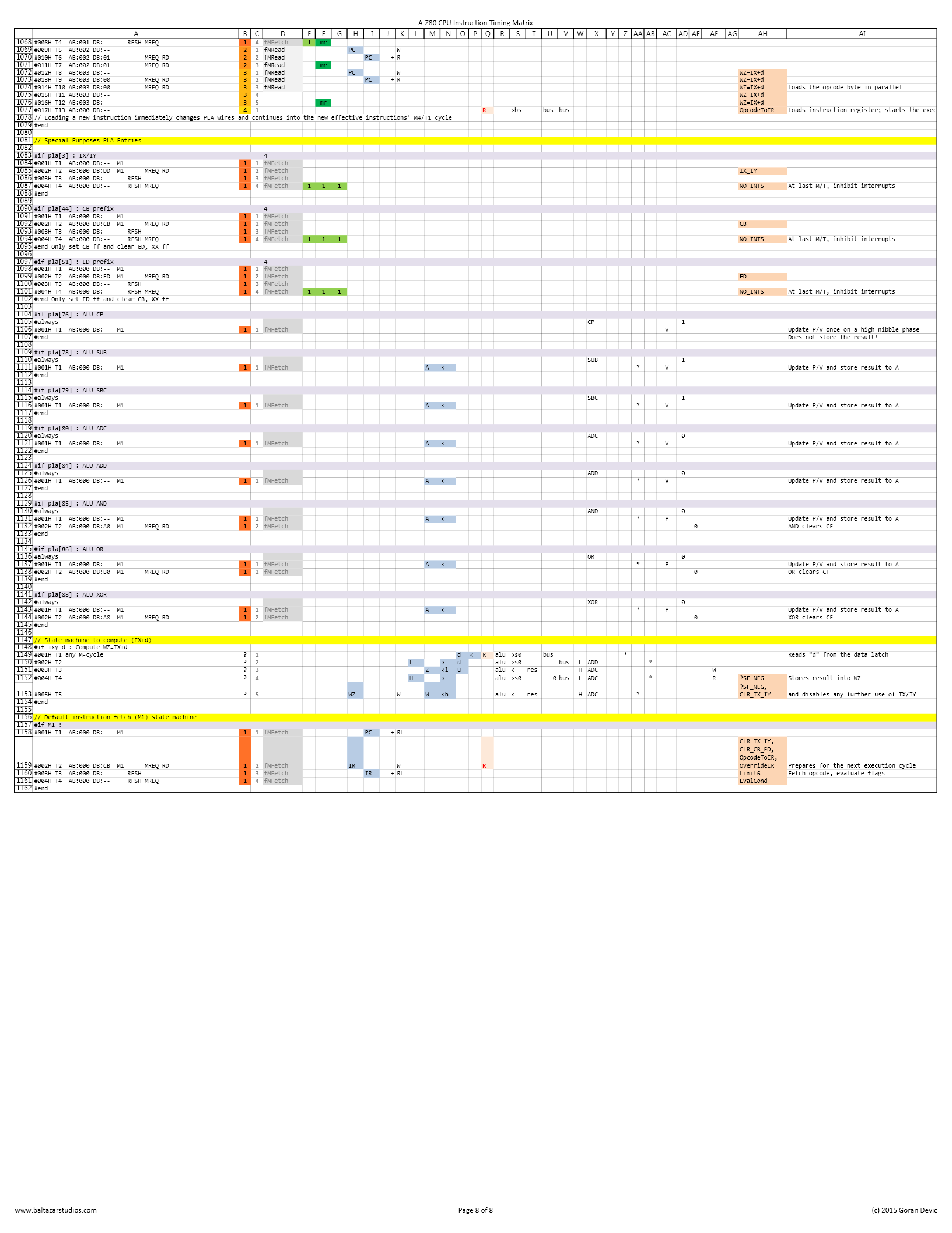
The most complicated task was to create the instruction timing matrix. Using all the information gathered in the process, I created an Excel spreadsheet with the exact timing of required micro-operations for each M (machine) and T (clock) stated of each opcode class.
This matrix defines the CPU and ensures it is fully Z80-compatible. In fact, if you modify it, you could create new instructions, enhance the CPU or even create a completely different one and the design would still just work!
The following set of images show the complete timing matrix printed from this XPS file. It is printed into 8 consecutive images; click on each to see it in full, readable size:
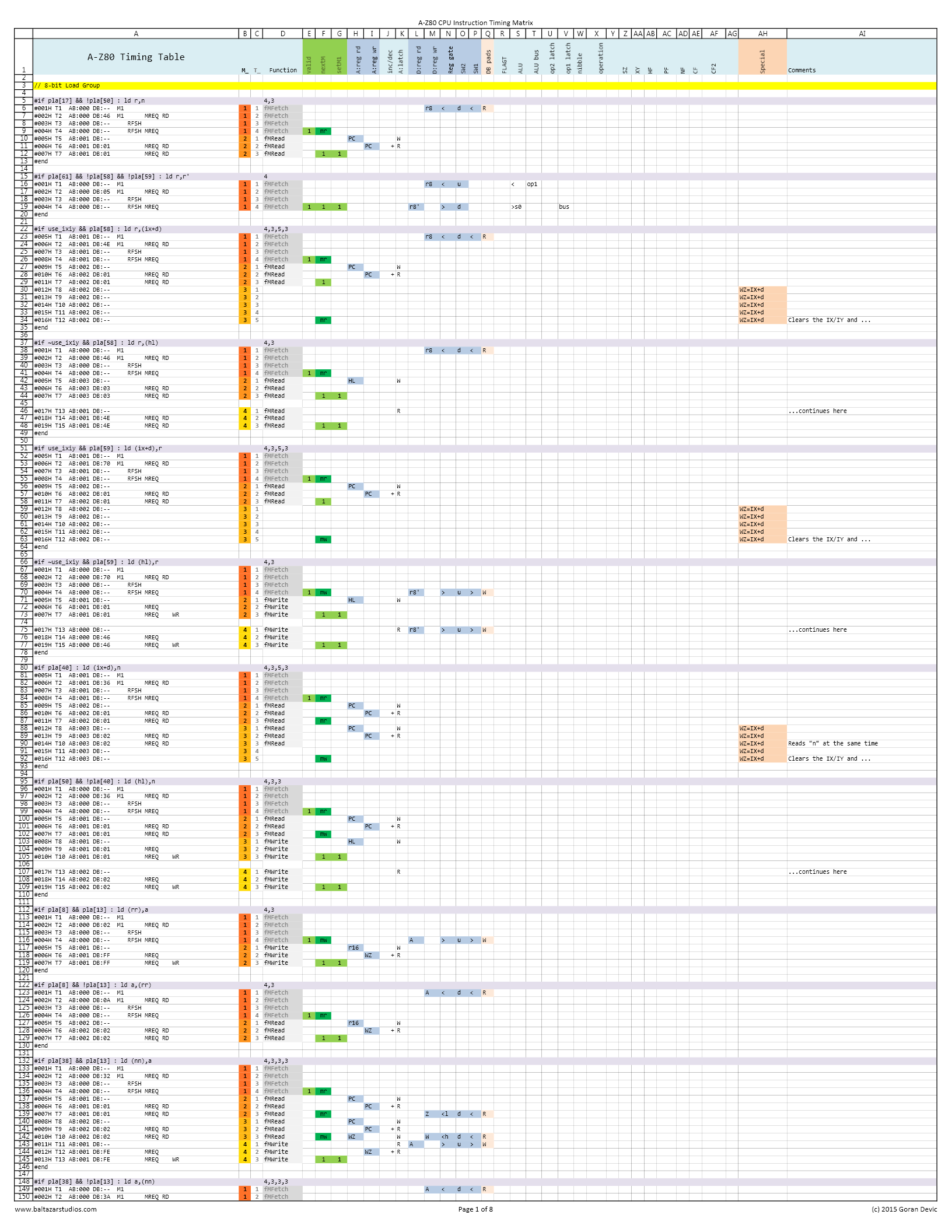
Timings 1/8
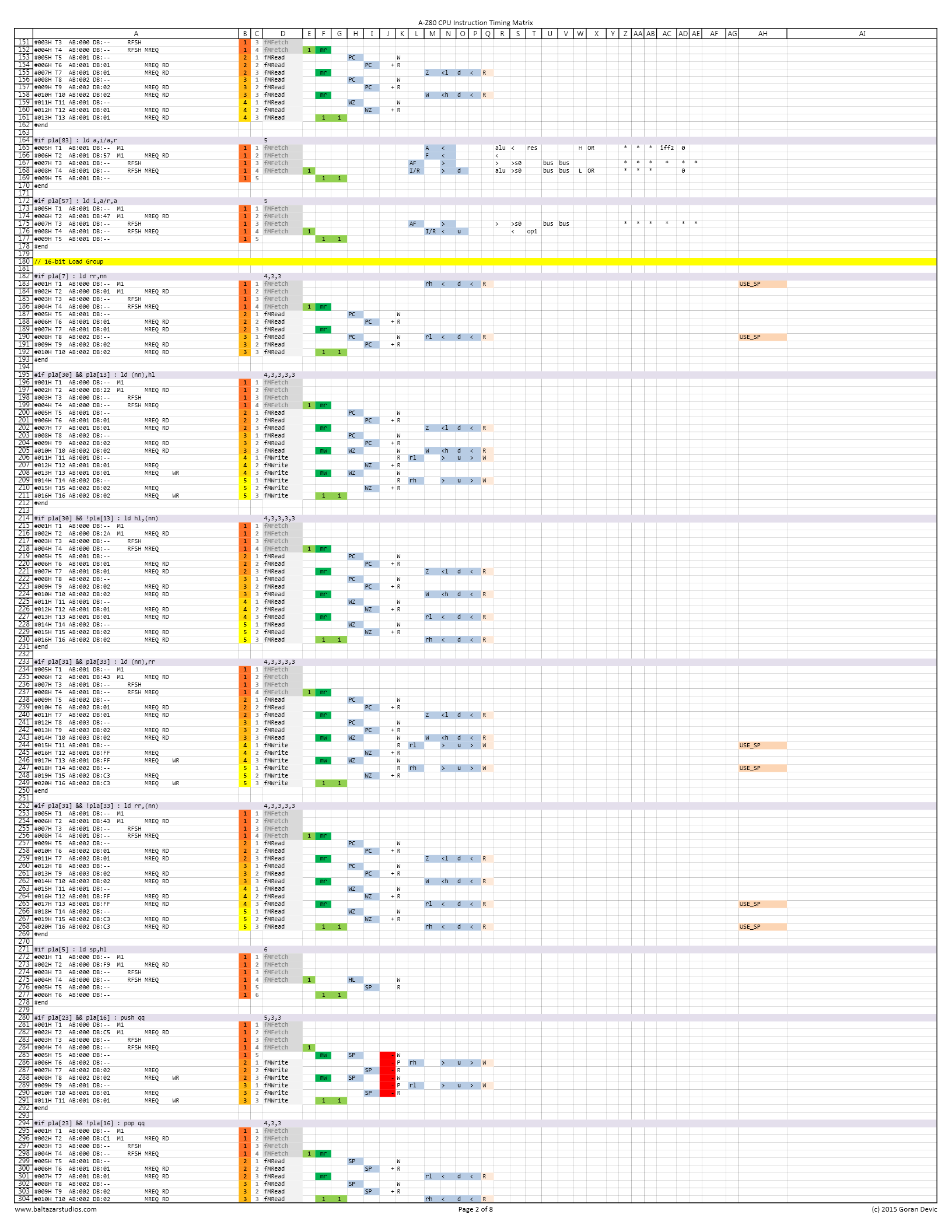
Timings 2/8
Timings 3/8
Timings 4/8
Timings 5/8
Timings 6/8
Timings 7/8
Timings 8/8
Each column, B through AH, contains zero or more micro-operations on specific internal design blocks (this file deciphers the tokens used). Groups of instructions are listed in a row as statically decoded by the PLA table, each line corresponding to a specific M and T cycle.
Rather early in the process, I devised several tests, including a full Fuse-based test suite that could run every instruction against a set of known results. That test proved the most valuable: it enabled to flag regressions as well as checking that the instructions were implemented correctly.
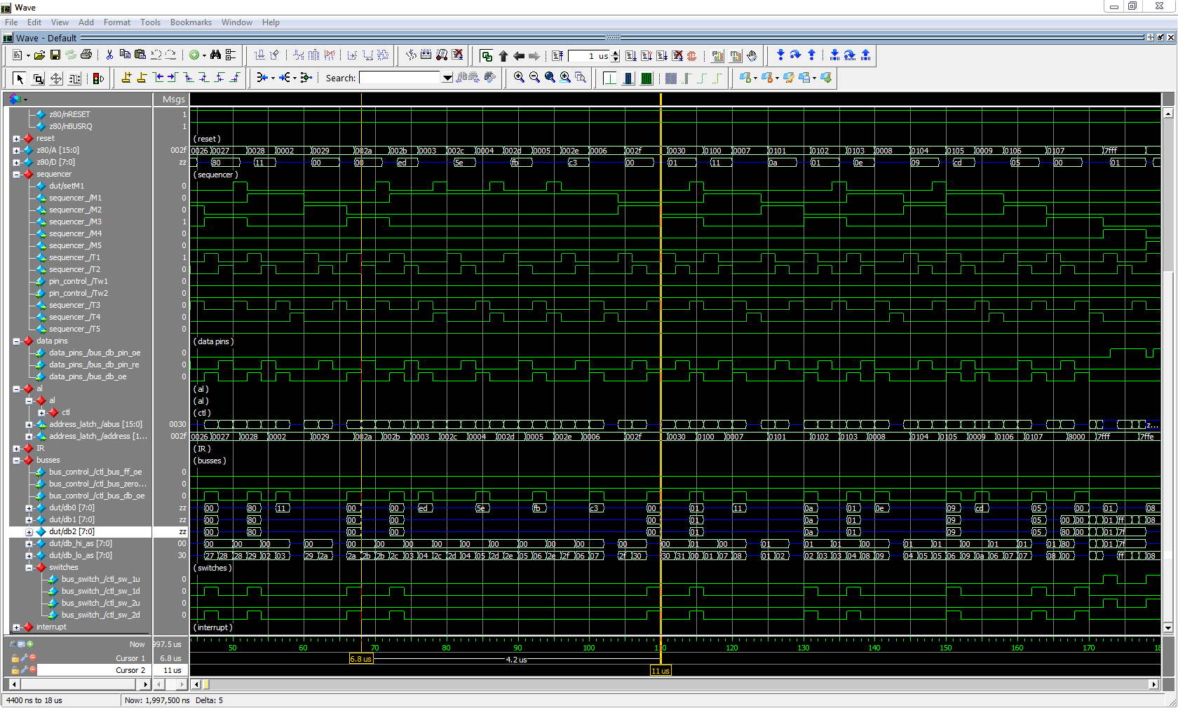
After some time, I was able to combine several Z80 instructions and run them in sequence. Enjoying many exciting milestone moments along the way, the one that stuck was when the PC register correctly incremented and was fetching successive instructions. They were also correctly executed since each one was tested separately: it all just worked!
After adding a virtual UART module in Verilog, I was able to get simple “Hello, world” programs sending the text out to a terminal! The same output would be captured by ModelSim simulating that code. It proved very helpful to have several different ways to test and correlate the results.
The most difficult part was getting the interrupt handling done just right. Z80 has 3 interrupt modes (im0, im1, im2), maskable INT with two flags (the enable bit and its shadow), and non-maskable NMI. INT is level-triggered while the NMI is latched, edge-triggered, and has precedence over INT. The pins should be checked at known times and be inhibited in certain situations, including during the execution of some instructions. It all needed to be working perfectly at known clock boundaries.
The solution ended up very elegant and used the minimum number of extra gates: besides necessary state flags and priority logic, it used a couple of control signals wired just right: see the timings page 7, lines 1028-1060, entry “rst p” and how the instruction RST38 is being used to handle both NMI and INT (im2) at the same time. You start seeing the beauty of the original Mr. Faggin’s design when you realize the coherence of the known behavior and the most optimal implementation. The simplicity of it became the proof of the implementation.
Once the CPU was wrapped up, it could run any code sequence using any instruction assembled and pushed onto a simple “board” model. That included some devilish and mean-designed interrupt-bombardment tests. It also runs well-known ZEXDOC and ZEXALL programs. They all passed except several XF/YF (undocumented flags) behavioral tests for 2 sets of instructions. Those are really weird and if you have ever played with Z80 emulators you would know what I mean. This particular Z80 behavior is likely a side-effect of internal bus charge/discharge cycles and some spurious control signals; various second-sourced and cloned Z80 chips also behave differently in these scenarios. I decided not to sweat over it as it had no practical impact.
Frankly, at this stage, I was already satisfied with the results since my original goal was to understand and replicate the internal architecture of the Z80, and I have achieved it.
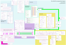
Compare the following image – a conceptual block diagram of the A-Z80 CPU – with the annotated image of a Z80 die from the top of this article to see the similarity in the layout. I have placed schematic modules at the locations roughly corresponding to their positions on the Z80 die. Not to scale. You should be able to trace major buses (data bus in green and address bus in red) and zoom into detailed diagrams to see gate-level implementations of the blocks. A few System Verilog sources appear just symbolically; naturally, the complete code would not fit on a printed page. Open it up in an image viewer that can zoom and pan.
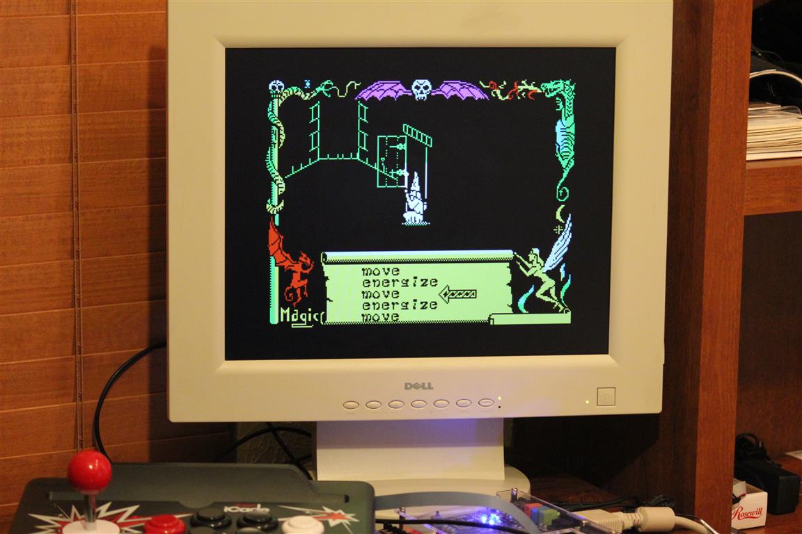
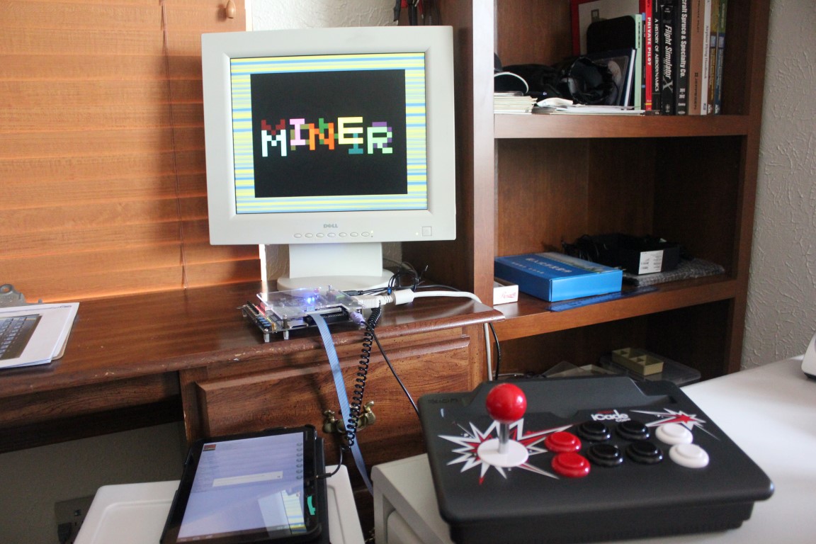
By that time, I was already fairly fluent in Verilog so the coding of a ZX Spectrum model was not a problem. First, I added a video unit by picking one (most suitable) VGA timing standard and was able to display static screens from various games. Then came the correct character blink and border behavior. After that: the keyboard interface, speaker, mic – all fairly simple modules. Once I got all internal mappings correctly set up, I powered it up, flashed it with the newest FPGA file and, to my huge excitement, saw a black screen clearing up and the magic “(C) 1982 Sinclair Research Ltd” prompt on the screen! I can’t tell you just how exciting that moment was; I kept resetting it over and over just to see it appearing again!
Soon I was able to load and play games!
But, there was one problem: the design would randomly reboot or lock up. I spent a long time debugging it but a chance conversation with Ed (a co-worker of mine, Ed is a world-class chip designer who really knows this stuff) would reveal a possible problem: trying to follow the exact Z80 architecture, I have used transparent latches in my FPGA design throughout. Well, no FPGA designs use latches these days. Ed told me a latch design would have never worked [reliably]. Well, I did make it work, somehow. Kind of.
Back to the drawing board and one month later, I have re-implemented the whole design to use flip-flops. Accordingly, I also had to modify a few timings here and there. The new design is fully synchronous and meets all timings; it is being checked using the TimeQuest static timing analyzer tool and has fully constrained timings (using SDC files). In the meantime, I’ve also found and fixed several issues including one important bug fix in the instruction timing matrix – I speculate that this fix alone would have most likely had solved a random hang issue with the latches (so the latch implementation would have likely worked well), but I have never gone back to check that. The final design is rock-solid to more than 18MHz (depending on various factors). It’s open and free for anyone to use; I uploaded it to OpenCores and the complete User’s Guide is here.
The lessons? I have learned a great deal of how to design, simulate and test a (small) microprocessor and work with FPGAs; I understood the Zilog Z80 inside-out by breaking it up into pieces and then re-assembling it from scratch; but most importantly, this ZX Spectrum implementation plays all 48K games I ever wanted to play again.
I would recommend a similar endeavor to anyone curious enough to undertake it for your own benefit. If you are one of those, please email me and we can connect and if I can be of any assistance along the way, I will gladly help you, in the same way, I got helped.
Note: This article was updated in 2016. In the meantime, I have ported all SystemVerilog files to Verilog and did modifications needed to use it with Xilinx FPGA tools. The A-Z80 CPU is being used by some retro boards such as Mist board (link) and the port to a few other boards is in progress.
To support loading ZX Spectrum games, I have also written an Android app PlayZX.
A-Z80 in more detail…
This project is part of the:
Hey Goran, nice to read a new post from you. Genious as always. I ended up opening a blog to discuss the work I did in one custom Z80 part used in arcade games. Take a look when you can: arcadehacker.blogspot.com
Rock solid up to 10MHz… have you tried it at faster clock speeds and had failures?
Just wondering, as I currently have a user-programmable CPU speed on ZX Prism up to 51Mhz
Cheers, Jeff
I did not do a more extensive performance characterization, let alone tuning. I know that 50% penalty is due to data/address pin latching on opposite edges – and that was a compromise I had to make to port it from using latches to using flops. If that’s changed, certain bus timings would be 1T off (instead of 1/2T) but fMax would be ~20MHz.
The goal was not to have a super-fast Z80 but an accurate reproduction of it (as much as it’s feasible) including being able to “see” Z80 internals at the schematic level. (People needing a fast soft-cpu have many alternatives!)
That said, it might be interesting to (1) tweak the arch and intentionally deviate from Z80 bus timings (or add delays) just to see how fast it can be made to run, and (2) have an original, latch-based version.
I’m currently trying to port the a-z80 to a lattice FPGA using icestorm tools, and I’m running into some issues with getting data_pins.v mapped (tool thinks that dout has mutiple drivers). What is that module supposed to do? I can’t seem to get my head around what that module does..
data_pins.v (generated from data_pins.bdf which is a Quartus schematic file) contains D[7..0] gates, it is an interface to the outside world for data bus. D[7..0] are bidirectional pins, don’t know if and how Lattice toolset deals with bidir wires.
replaced the code with
seems to map properly now.
Thank you for the fix! I will update the code.
Best Regards,
Hi Goran, MP,
I am also having issues when synthesizing A80 for Lattice FPGAs with Yosys, (icestrom), my issues are:
Did you guys had same experiences as me?
MP, please may you post your complete data_pins.v file? I can check if that fixes also my issues.
Regards
Juan
New data_pins_lattice.v code has been pushed to BitBucket
The export.py file has been modified to notify of this special case with the Lattice toolset; for now, simply remove data_pins.v and use Lattice variation.
Unfortunately, I don’t have a Lattice setup to check; I could get a board from eBay, but not sure about the total cost of all the tools. Right now I do verify every change on Altera and Xilinx (and also people email me as they are using various boards but it has been only Altera or Xilinx up to now).
Hi Goran,
If you are thinking in buying a development board, make sure to use the “iCE40-HX8K Breakout Board” at minimum. Please note that they are really small FPGAs, a A-Z80 takes about 50% of the resources on that hardware.
About the tools, the ones I am using are free! I follow the guide for APIO Framework (https://github.com/fpgawars/apio)
Please do not hesitate to contact me if need some support.
Did you have any other issues with the Lattice toolset and this code?
I am adding it to the documentation and your code to the release as a Lattice special case.
Thanks!
Hi Goran,
Sorry, I forget to really thank you for so excellent work. It is really cool and a reference for me. I am a rookie in RTL, so maybe in my following lines you may find some mistakes.
As I wrote before, I cannot simulate properly write cycles using your lattest sources and nor modelsim or IVerilog/GTKWave simulators, I always have the same issue, undefined address bus values on write cycles.
I made the following top module using your CPU:
And this testbench:
And, also wrote a simple assembler application that spins as follows:
It is clear that the processor executes properly fetch cycles, and I tested also read cyces, but with writes the processor always places address bus to undefinted. I have a bitmap that could upload with some help.
Thanks for your support
Juan
(oops, sorry formating didn’t work as expected1)
Hi Juan,
Our posts got a bit out of sync since I have to manually approve each, otherwise I was getting tons of spam. Likewise, I manually edit each post (incl. yours) for source formatting, so don’t worry about that.
Would you mind we move our conversation to email? It would work better until we resolve your issues. Please email me at gdevic at yahoo com
Everything that you mentioned so far is still using Lattice toolset, right? I test on both Altera and Xilinx and those have no issues synthesizing. If you could advise which Lattice tools to donwload (free, I hope), perhaps I could repro some of the things you see, at least the simulation part. Hope the learning curve on it is not too bad…
I run ModelSim (Altera edition) extensively, though.
Thanks!
Wow, brilliant!!!
Hi, Goran
I am trying to compile your core (downloaded from GitHub) and am getting many errors like this:
275022 Illegal bus range or name for logic function for instance “alu_” of type 4-BIT ALU CORE UNIT
My usual language is VHDL, so I don’t know if this a real problem with the files or some Verilog thing I don’t know about. I would appreciate any insight you can provide.
Also, the top level files for the hosts are not in your GitHub files. This is not a problem for me since I can easily interconnect them, but it might be a problem for others.
Thanks
Jeff
Goran – I forgot to say I am using Quartus V13
Jeff, I am using “Quartus II Version 13.0.1 Web Edition” for Altera Cyclone II device on DE1 board. I just double checked and all files should be there. Did you try to load “https://github.com/gdevic/A-Z80/blob/master/host/basic_de1/basic_de1.qpf” for example?
You can email me in private and I will try to help you.
Hi!
I’m implemented this core to my test project and have one error:
Error (15856): Output port O of I/O output buffer “pre_syn.bp.vm_addr_0_~output” must drive a top-level pin
and same error for others address pins.
I’m copy all files via export.py and add to project. Example projects compiled succesfully…
If delete connection from core to address bus – error dissapear.
Hi Andreil, are all Z80 pins connected to other modules in your FPGA design? I’ve seen this kind of error if I did not connect some of them. Usually, they drive internal address bus which is shared with some ROM/RAM cells or similar.
Hi Goran,
Amazing work!
Just one issue – it seems to ignore port reads while everything else works, i.e. keyboard port – ZX spectrum works, but ignores an input from a keyboard. For example in this code it never arrives to the line “led <= 4’b0010;”, I even removed all other conditions. Just wondering if you’ve seen this issue before?
Hi Alx, no, I have not seen any issue, on my board(s) it all works. Can you tell me which board and tools are you using to synthesize it? If you want, you could email me in private and we can try to figure it out since it should work.
Hi Goran,
I would like to apologize, my “real” ZX spectrum knowlegde is more than 30 years old, and I completely forgot that nINT is required for keyboard to be polled. After I implemented this logic everything seems to be OK. There are some minor quirks I would like to discuss over email, probably they related to actual FPGA but may be not, mine is alxlabs at gmail com
Just for statistics:
1. I implemented everything but actual Z80 myself, bit thanks to you for sharing your work!
2. Im my design I use USB keyboard, not PS2
3. I don’t mind sharing everything 🙂 just ask me if you like to see my code/schematics etc
4. I use Cyclone IV, Altera ALINX board
5. I use Quartus II 64bit 13.0.1 build 232. I also tried to use Quartus Prime 21.1.0 build 842 – results are same.
Thanks a lot,
Alex.