Z80 Explorer is a Zilog Z80 netlist-level simulator capable of running Z80 machine code and also an educational tool with features that help reverse engineer and understand this chip better.
(Updated on 9/11/2024)
Z80 Explorer is a tool I wished I had a few years ago when I first started looking at the photos of the Z80 chip die and was learning to reverse-engineer its features. The process was slow and painful as it involved deciphering the faint image traces into logic gates and functions.
Sometimes later, I found that the Visual6502 team has done wonderful work mapping the CPU’s traces into bitmaps representing various layers. Their online viewing tool is impressive, and one can learn much from it. Like most online tools, it has limitations, which I quickly hit when trying to understand the chip behavior more deeply.
My wish list of additional features steadily grew as I kept playing with the online tool. I would have wanted it not only to be a fully functional and fast simulator but also to provide more elaborate ways to gain deeper insights into the chip’s internal behavior while also being educational, easy, and intuitive to use.
Fast forward to today, and with the help of repeated COVID-19 stay-at-home orders, I have written this tool to be how I initially imagined it.
In this blog, I will give an overview of Z80 Explorer‘s capabilities and show some valuable features that might be easy to miss even after reading the documentation. This blog and the tool may change periodically as I update and use it.
The tool’s user guide is a separate online document: Z80 Explorer Guide. It is concise; if something is unclear, please email me, and I will explain it better.
The tool uses the Z80 dataset (layer images and netlist). It should be able to accommodate other NMOS chips with minimal changes. However, at this time, I haven’t done any other ports yet, as I was solely focused on Z80. The chip’s data (resources) are kept in the resource folder. In particular, as the functions of various nets are better understood and the nets and buses get named, the list of the net names, tips, and annotations can grow and be shared.
Z80 Explorer is capable of running native Z80 code at the netlist level. That means as the instruction opcodes are fed to its pins, the binary 1s and 0s propagate through its internal nets of transistor gates and perform the function identical to what the silicon gates would do on a real chip.
The engine that runs it is pretty fast: On my original 4GHz i7-4790K CPU, when I initially wrote it, I could run Z80 code at around 2.3kHz, which is (only!) around 2000 times slower than the speed it would run on real silicon. My new PC, Intel i7-13700K (5.3 GHz), simulates it at around 4.1kHz. That is about 1000 times slower than the real chip.
At those “speeds,” it is not inconceivable to run some of the standard CPU diagnostic programs – so I did just that: I ran a well-known ZEXALL diagnostic program.
That program typically takes hours, even on a real Z80.
After a few days of running within the simulator, the list of passing tests kept growing.
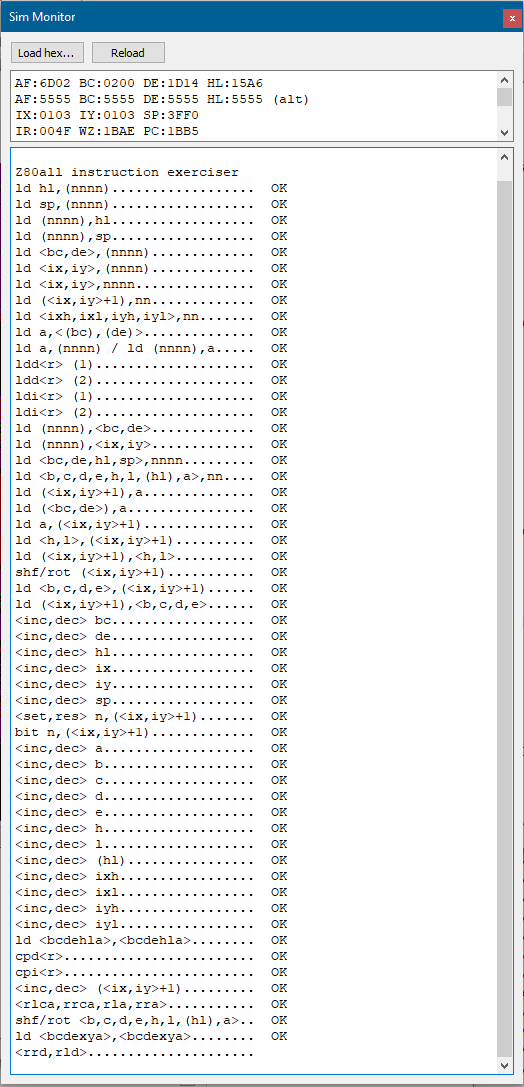
I have added that version of ZEXALL to the app resources. It is modified from the original in that I sorted the tests by how long they run: with the quickest going first, it does not take too long before you start seeing some results, assuring you that it is running well.
Z80 Explorer implements “Image views,” which show various versions of chip images. Some of them are unmodified resource files shown as layers (diffusion, metal layer, etc.), and some are created as combinations of those; for example, “vss.vcc.nets.col” is a layer combined with the nets colored such that ground is shown as green, VCC as red, and the rest of the nets are colored according to the user-specified filters.
You can view different layers and create layer combinations if you hold down the Ctrl key while clicking on layer buttons or press a key assigned to each layer while holding down the Ctrl key.
The chip/layer view can also be annotated. At the start, the application loads a default annotation file, but you can load any other annotation file by dragging and dropping it into the application image view. For example, “annot_internals.json” (also located in the resource folder) contains different annotations focused more on internal features. Annotations are adaptive, so their text will show and hide as you zoom in and out of the image. They also can contain macros, tokens that expand into named net and bus values, updated in real time as the simulation runs.
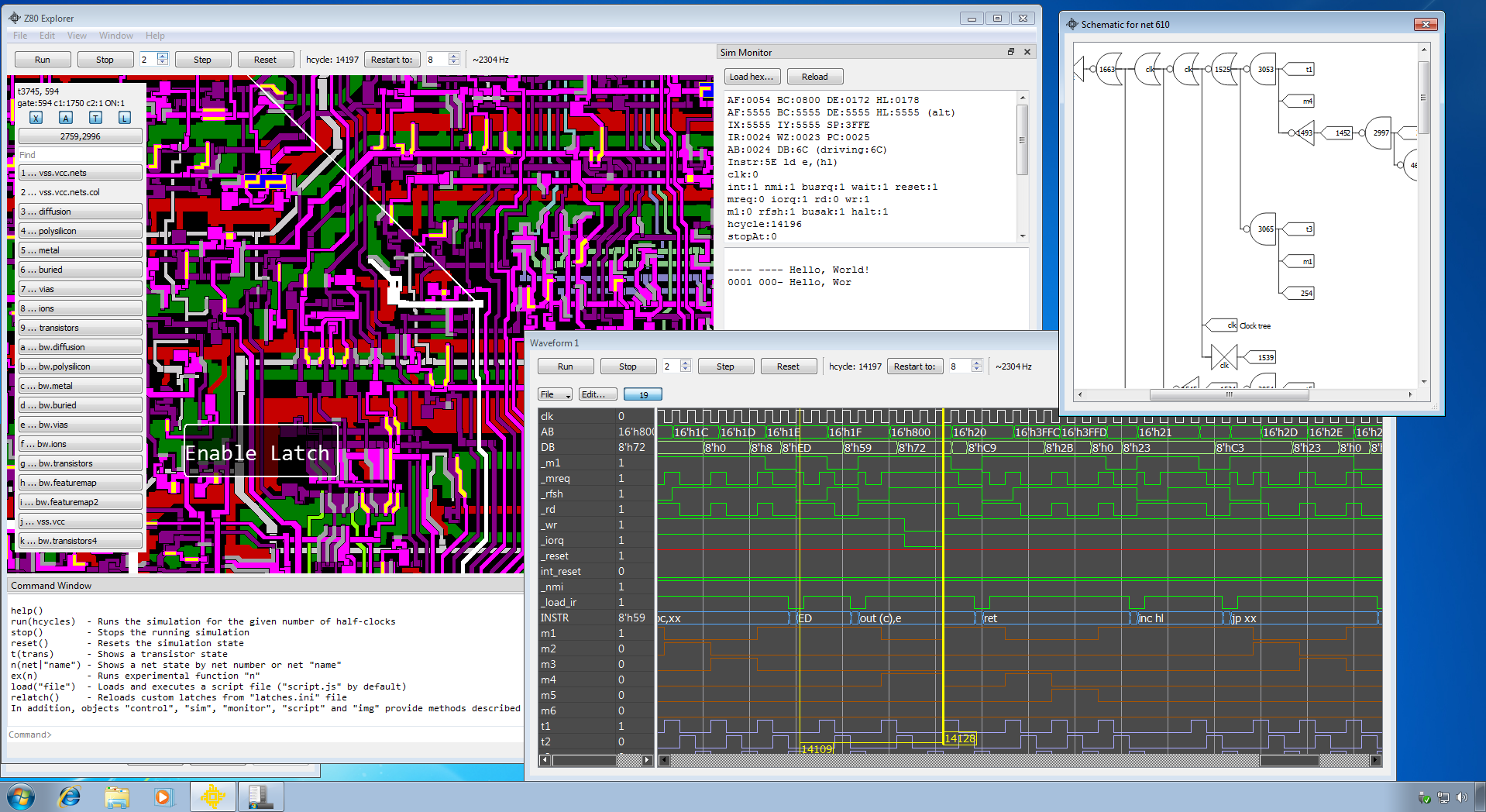
In my older article here I looked at the Instruction Register. The signal that enables loading is a complementary WE (Write Enable) pair of control traces.
Can we find precisely at what time(s) the write enable, now called “load_ir”, is asserted? What is the internal logic equation that governs this control signal?
Using the Z80 Explorer‘s “Find” option to search for the “load_ir” signal name and then asking for the schematic of that net brings up this view:
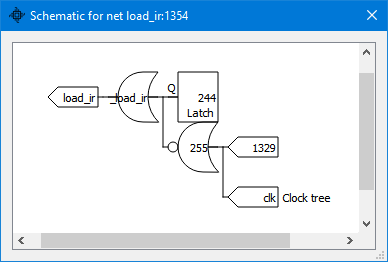
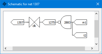
Hence, the signal is generated by OR’ing net 255 with a latch. Let’s follow net 255, a NAND gate of the clock (hence, a clock gating), with net 1329. Selecting (double-clicking on) 1329 and asking for the schematic brings us even closer to what we expected to see:
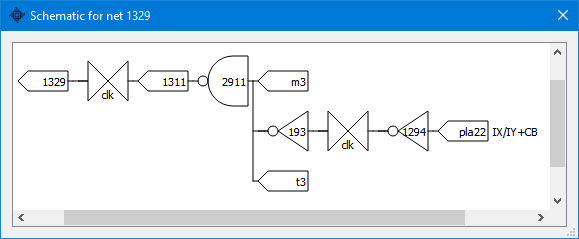
Therefore, net 1329 is a clock-gated, NAND-combined signal, active when M3, T3, and PLA22 are active. PLA22 represents “IX/IY+CB” instruction extension decode. (The description of PLA22 is in the application “tips” file, as are descriptions of all other PLA entries and other essential nets).
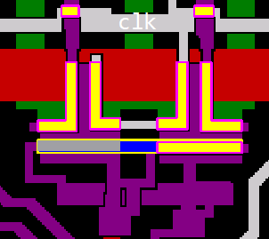
Back to the latch 244 – and this part may not be too obvious unless you have some experience looking at the chip traces – the net 244 is at the bottom, and the latch set and reset signals are at the top, both clock-gated:
Asking for the schematic of net 1306 (the one connected from the top-left), which also acts as the latch reset:
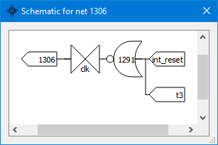
we see that the latch will reset on the “internal reset” or a T3 cycle. The latch will be set on an M1 and T2 cycle edge (so it will show at M1/T3):
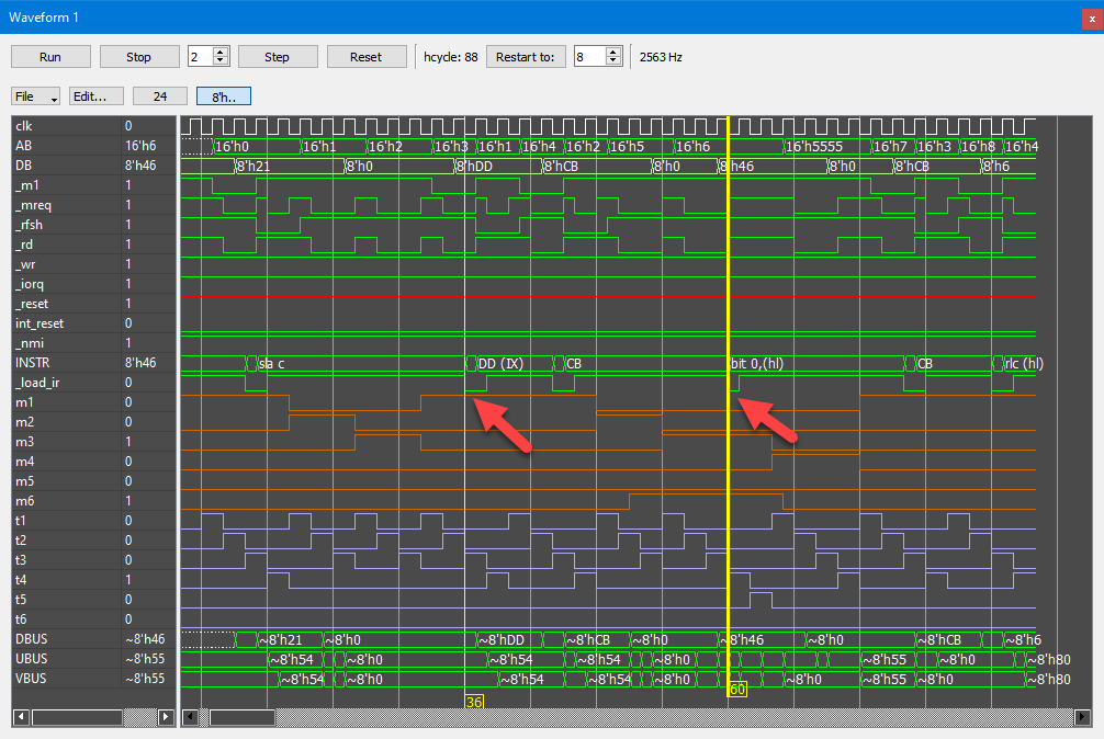
We can verify what we’ve found by running a hand-crafted test code. I used a template test program “test_blank.asm” to code in a couple of instructions, one using IX register, and then I ran it for a couple of cycles. In a Waveform view window, the result shows how the load_ir signal is being asserted at every M1/T3 and at M3/T3 when the instruction is using the IX/IY prefix (PLA22 active).
Next, load the “annot_internals.json” file by dropping it onto the application’s image view (the main pane).
You can zoom into the area where are all M and T latches located by pasting this command into the Command Window:
img.setZoom(0.98); img.setPos(1151,901)
On the startup, the app will try to detect latches, and it will detect most of them automatically. You can add those that have not been detected as you find them. The easiest way to find latches is by using the “Driven by” option. After selecting a net and following its signal chain, if you see two nets being driven by each other in a co-dependent loop, you have found a latch consisting of those two nets (also acting as inverters). One of the app’s initialization files, “latches.ini” contains definitions of additional latches. You can add to that file as you find latches that the app did not detect.
The schematic view uses an expanded version of the “Driven by” algorithm to build a tree of gates contributing to the selected net.
Going the other way, the “Driving nets” option assists you in tracing an input net as it branches into the network. For example, pick the /RESET input pad and iterate “Driving nets,” following the highlighted lines. Soon, you should reach a “dead end,” with the nets, which apparently nothing is driving here:
img.setZoom(2.926); img.setPos(338,606); img.show(294,548,80,101)
About these commands: To create these zoom and position commands yourself, set up the desired view and then type “img.state()” in the Command window. The required lines will be printed in the Application Log window.
To obtain the coordinates used in the img.show() command, right-click and select an area you want to highlight, and then simply read the coordinates from the Log window and paste them into img.show() as arguments.
The particular network mentioned above contains reset input flops and latches. One of the control signals coming out of it is “int_reset,” or internal reset:
img.find("int_reset")
This signal branches off to different parts of the chip.
Every chip normally has several signals propagated across its die to every corner. Some of those networks are power, ground, reset, and clocking networks. (Newer chips implement various “gating” in parts of the design to limit the power consumption, but Z80 does not do such a thing.)
I have already mentioned the Waveform view. This view should be familiar to anyone who has worked with simulation tools like ModelSim; but it should still be straightforward and intuitive even for the rest.
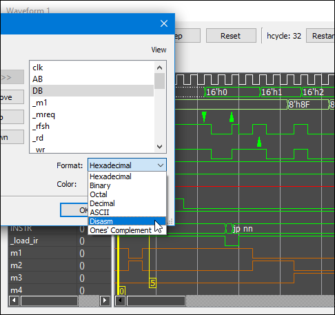
Remembering to “name” the net you wish to observe is critical. You can not add it to the waveform view if it hasn’t been named. Double-click on the net and select “Edit net name…”. You can type any name; a simple “n123” (where 123 was its net number) would suffice, especially if that is only a temporary net and you do not wish to keep it. You can always rename a net later if you’ve found a more suitable name, or you can delete the name.
The resources’ “tests” folder contains several Z80 code snippets. Some of them can be assembled and run as-is (“zexall.asm”), the others contain code to test specific functionality (“test_busrq.asm”) or are there to serve as a template for your experimentation (“test_blank.asm”). They can be built with a provided Z80 assembler (zmac.exe).
As you run different Z80 code snippets, you can see how selected nets behave in various scenarios. You can deduce what a signal does once you analyze its waveform.
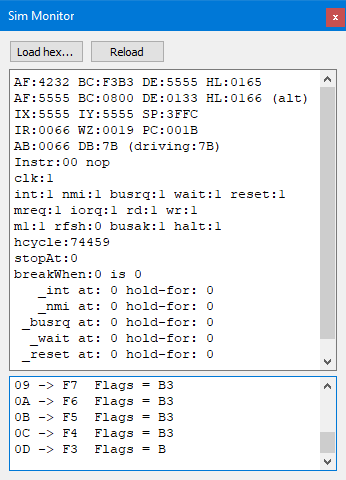
Some of the “advanced” features of the app let you set up many specific conditions for observation. For example, you can set up and see what happens when the NMI is asserted at a particular clock cycle. You can modify the test programs and set up your conditions by writing to the “trick box,” a simulated memory-mapped area. These address locations are considered “special” by the Z80 Explorer’s simulation engine. Writing to them will cause various events: injecting an interrupt at a particular clock, holding the reset pin, releasing it, etc.
(test of NEG instruction, in this case)
By carefully crafting a test, you can set up a quick, repeatable, and convenient simulation cycle and observe what the signals do and how the chip behaves. In addition to net tracing, schematics, and annotations, the software should provide a sufficient framework to understand how Z80 works internally.
A single blog can’t cover all the features that this tool provides. I have not yet described the Tips feature (which lets you tag nets with additional information like those that describe each PLA line), custom colors for groups of nets, embedded JavaScript engine and scripting commands, and the “trickbox” memory area used by the simulation monitor to control the test programs and how test programs can control their simulation. However, the documentation briefly describes all those features with enough detail to provide the necessary guidance.
To conclude with something slightly different, how about booting a ZX Spectrum within this simulation?
For that to happen, I executed this external JS script file. I have also provided the 48.rom file.
mon.loadBin("48.rom", 0);
mon.rom = 16384;
mon.enabled = 0;
mon.zx();
reset();
run(0);
About 20 minutes later…
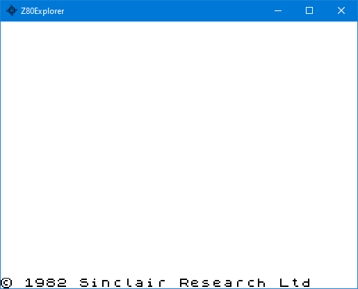
The script to run this demonstration is “zx.js” which you can find in the app resource folder.
Although many portions of the Zilog Z-80 CPU have been reverse-engineered (see excellent Ken Shirriff’s articles on Z80), many parts are still unknown or poorly understood. I hope this tool will allow the curious to finally completely understand the Z80’s inner operation.
Happy and fruitful Z80-exploring!
You can find Z80 Explorer at Github: https://github.com/gdevic/Z80Explorer
There is also a YouTube video that shows it in action: https://youtu.be/_dyngzTEnvw
Note: This post has been updated on September 2024 to match the new Z80Explorer version 1.05
The link to the Z80 Explorer Guide, “https://baltazarstudios.com/Z80ExplorerGuide/” goes nowhere as of 7/22. Did you pull it down to make changes? Can’t find it anywhere on your site or on the Github.
Fixed. Thanks for pointing that out, JRD!
Thanks Goran, you just made this summer the program I was looking for ! I didn’t even remember there was a Visual Z80, it doesn’t appear as link on their homepage…
By the way, your program is really useful to understand the Z80. The only think I would prefer is having a vector view that directly uses the netlist points to display polygons (like the Visual 6502 team did in javascript). You chose to use PNG layers like in the Intel 4004 emulator, and of course the problem with bitmaps is that you can see pixels when zooming, so you don’t see clean polygonal shapes like in the real chip die.
I hope you will continue to work on Z80 Explorer and I will follow this project closely 🙂
Olivier
Although I’m not much of an hardware expert, this is extremely cool!
One question popped to my mind: Many Z80 documentations talk about IFF1 and IFF2 while explaining INT chaining. How do I find them from this simulation? I would like to add them to watchlist.
I would probably start by enabling latches in the view (“L” key) and then trace back from the INT pin and keep adding all connected latches to the watchlist; rerun some test(s) designed to exercise all known IFF1/IFF2 states (we know how they should behave in specific situations) and then see which latches match the behavior. Alternatively, trace back from the INT pin and try to understand what the chip does with it. Sooner or later, it will hit those two latches.
Another way would be to issue EI/DI (which set and clear IFF1). Tracing those instructions will lead to IFF1. IFF2 is a temp storage for IFF1 when NMI happens, so they are likely close to each other. Also, there are instructions that load IFF2 to parity flag; tracking them should reveal where that bit is coming from. RETN also touches IFF1/2, stepping through RETN could show where that flag gets loaded from.
Another question…
On test_proto.asm there is:
; IM2 vector address and the handler (to push 0x80 by the IORQ)
How ever it is unclear to me, how can I push a value to databus during INT? There does not seem to be address for it in trickbox.inc
Good catch! I don’t think that’s currently possible. It’s definitely something that would be useful. I will see how to add it.
Seems that I forgot to thank you that you fixed this issue. All of this is absolutely mind blowing stuff. Z80 production was now finally halted (june 2024), but your work will help a lot of people for a long time to the future. Thank you!
This is a most amazing and impressive tool for anyone wanting to better understand Z80 internals.
I was most impressed that your sim passes zexall, meaning it correctly sets and clears the undocumented X and Y flags (bits 3 and 5 of the F register). I’ve not been able to get my Z80 sim to pass zexall’s “bit n, (+1)” test (it passes all the others), as that test requires my sim to correctly set the internal WZ register (MEMPTR) for every instruction that makes use of it. (I’m still trying.)
Of course, why *wouldn’t* your Z80 sim correctly set the WZ register—it operates at the die/gate level. Your sim doesn’t need to know the details of the Z80 registers or how/when they are set; only that the Z80’s die/gates are simulated correctly (no small feat!).
I’m looking forward to playing with Z80 Explorer, as I’m sure it will offer me insights that will help improve my own sim, and hopefully help my sim finally pass zexall. ?
Kudos to you for this outstanding piece of hardware and software engineering!
I can’t seem to get ex de, hl to work. I modified the hello world code as below, but the output does not show the E register changing, have you any ideas why? Great code btw!
org 100h
boot:
; Set the stack pointer
ld sp, 16384
ld hl,0
ld (counter),hl
exec:
ld c, 2h
loop1:
ld de, 00404h
ld hl, 0fefeh
ex de, hl
call 5
jr loop1
I can try to look at that this weekend.
Here’s a better example:
exec:
ld c, 2h
ld de, 00505h
ld hl, 0fdfdh
loop1:
ex de, hl
call 5
jr loop1
So it seems that the accumulator does pick up the modified e register correctly, but readByte isn’t noticing the updated values in the de and hl registers, and neither do they show up on the image view or monitor, which I am guessing are driven by readbit/readbyte?
Ah, mystery resolved, the z80 cleverly does not actually move the contents of the registers, and instead just sets some flags which are found in nodenames.js under EXX latches.
So this is an early ( first? ) example of registry renaming used in modern CPUs ?
interrupt mode 0 is supposed to accept any byte on the data bus as an instruction. the standard thing is to pass it a 0xCD or a reset instruction. what if you give it a relative jump? or an increment register? or a push HL? or, heaven forbid, a 0x21.
I believe the cpu follows a “regular” instruction fetch cycle at that point.
[…] Z80 Explorer […]