After reading excellent Ken Shirriff’s blog on reverse-engineering parts of the Z80 CPU, I decided to learn how to decipher some of the chip die-shots myself. It turns out not to be that difficult if you follow certain guidelines, which I will describe in this post.
Start with a good and clean die shot. Although the Visual 6502 team had a good one, it was somewhat grainy, and I’ve found a much cleaner version here. There is a slight difference in masks, but the functions are the same. In fact, it may even help to look at several versions when trying to decipher the layout.
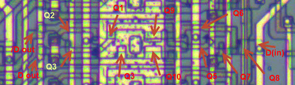
This is a side-by-side image of two different die-shots at identical places: the left one is from the Visual 6502 team’s website and the right one is from a Russian Z80 clone. They both show a portion of the chip we will focus on – instruction register latches.
The instruction register (IR) is located between the instruction decode PLA and the internal data bus. During the opcode fetch phase, the instruction byte is being read from the external memory and latched into this register. This is a transparent latch, and it will keep PLA wires active and stable until the next instruction is being latched in. PLA, in turn drives the execution logic (Z80 did not use microcode).
If we zoom into the image, you will faintly see the layers. It would have been easier to trace them if the top metal layer has been stripped, but in this case, it has not. Most of the metal wires are grounds and power (5V) and they are easy to spot due to their bright color. Since all active gates need those, they can be found combing throughout the chip logic. It is amazing just how much plain wiring there is compared to the transistors areas in these old chips.
Below the metal layer are polysilicon wires which are also used as conducting wires and usually run perpendicular to the metal. They form a grid for signals to travel. Vias connect those two and they are also easy to see.
A Transistor gate forms when a polysilicon wire crosses an active, doped region of the silicon substrate. Those active regions are hard to see, but they do have a faint edge caused by different oxide thicknesses created to mask when implanting ions into the substrate.
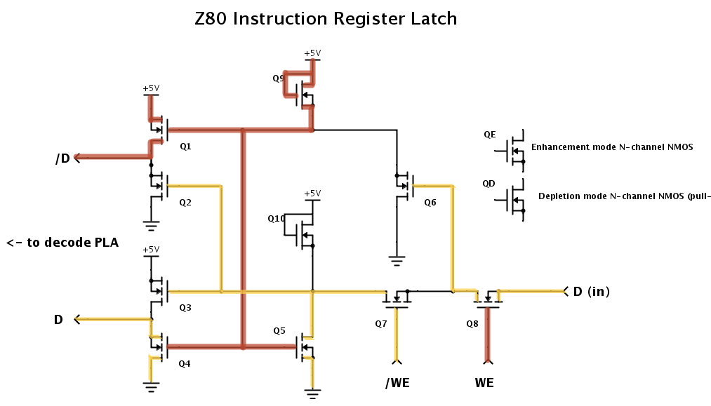
In the image above I circled a single bit of the IR latch. A bit of data enters from the right and on the left we have 2 wires coming out and into the PLA: one represents the unchanged bit and the other one is its complement.
Down to the technique – you may find your own preferred way and this method works for me: clip two transparencies over a printout of a die and use dry erase pens to trace active regions on one and poly wires on another. That way you can keep erasing and rewriting lines until you figure out the layout. Have doped region on its own page so you can erase its traces without having to redraw other wires – and you will likely modify doped region most since it is hardest to figure out.
Get the low-hanging fruit out of the way first: find and mark ground and power metal wires and all the vias. Separate regions that clearly only pass wires as opposed to implementing transistors. The next image should give you some idea of how these places could look like.
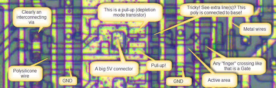
A couple of tricky points here: active regions can also be used as interconnecting wires at “short” distances (see the one pointed to at the bottom-right corner). Big square blocks around power metal wires are usually depletion-mode transistors acting as pull-up resistors. Small fuzzy rectangles around a poly wire usually connect that wire with an (active) base forming a continuation of a wire. Transistor does not form at these micro-vias exactly because of that particular doping to prevent it – the one helping us to see that transition!
Once you have traced the layout correctly things will start making sense. There definitely is a mental jump from having a region layout to just seeing the transistors, but trust me that if you look at it long enough it will be increasingly obvious what it is 🙂
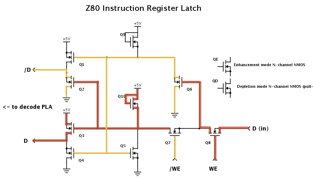
This diagram shows the latch when a bit of “1” is being latched in. Two wires from the bottom are “write enable” and its complement. When WE line is asserted, a bit “1” (drawn in red color throughout) is being latched into transistor Q6. Negated WE wire keeps it separated from the rest of the logic at this time.
When the WE line is cleared, the latch remains in a stable state due to the feedback loop between Q5 and Q6 (which are two inverters that latch a bit). Remember that in NMOS technology signals would like to be “1” (pulled-up) unless something (one or several transistors) are connecting them to the ground. Hence all yellow lines represent ground propagation by a closed pass-transistor.
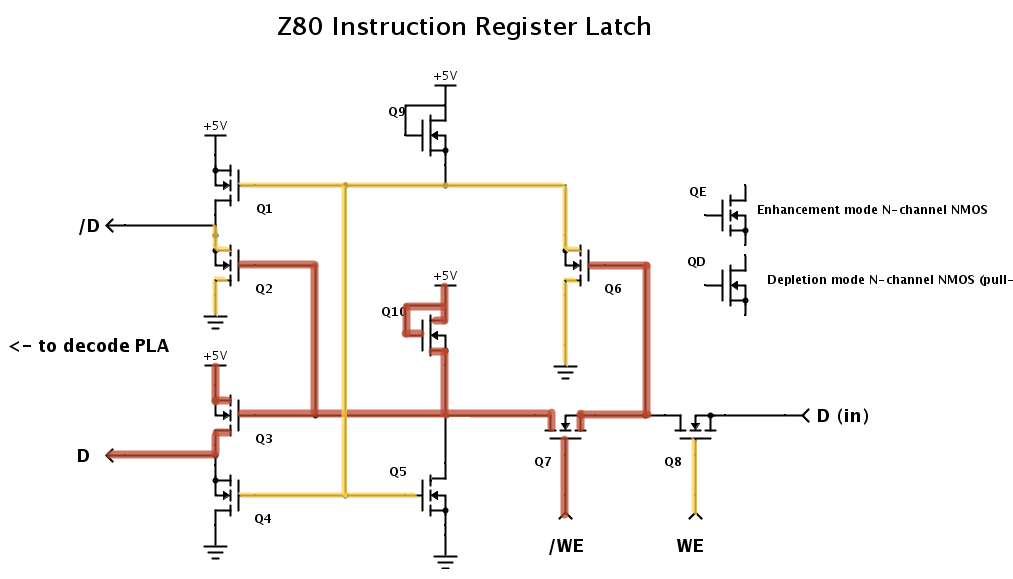
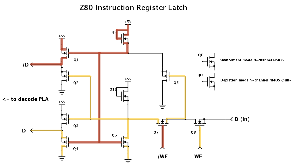
Similarly, we can see the signals when “0” is being latched from the data bus:
and also after it has been latched:
Q9 and Q10 are depletion-mode transistors and Q1 through Q4 are output drivers in push-pull configuration.
Although Z80 is an old CPU, it has been manually laid out by two geniuses: Federico Faggin and Masatoshi Shima. Today we would call it an all-custom-cell design. It is both challenging and exciting to get a glimpse into their world and a very exhilarating feeling once you figure parts of it out.
Additional reading:
- Guide to reverse engineer silicone gates (PDF)
Sources of Z80 images:
- Zeptobar’s images of various editions: KR1858VM1 (Soviet Z80), Z80A, Z0840004PSC, T34VM1
- Visual6502 Team’s FTP site
Hi,
BTW if you need photo of T34VM1 or Z80 with stripped metal – I can do that to help with your research.
Best regards,
Mikhail.
Mikhail, having a stripped metal photo would help tremendously! I like working from the Zeptobar’s photo of that particular clone not only because it is much cleaner and crispier than what 6502 team has, but also I believe T34VM1 might be free of traps that Shima/Faggin put in all their formal Zilog editions. Can you contact me at gdevic at yahoo.com email? Thanks!!
The link to ReActiveMicro’s PDF does not work. It appears that it is now at https://downloads.reactivemicro.com/Electronics/Reverse%20Engineering/6502%20-%20Guideline%20to%20Reverse%20Engineering%20v1.0.pdf
(Electronics/ has been moved from Public/ to the root directory, and Public/ no longer exists)
Thanks, I have updated the link.
[…] my older article here I looked at the Instruction Register. The signal that enables loading is a complementary WE (Write […]