The data bus on the Z80 processor is 8 bits wide. Data bus wires carrying information within the chip itself do not simply connect to package pins and out to the world – the gate circuitry of each bit is quite complex. This article presents a transistor-level schematic of a data bit’s gate which I reverse-engineered from a die photograph.
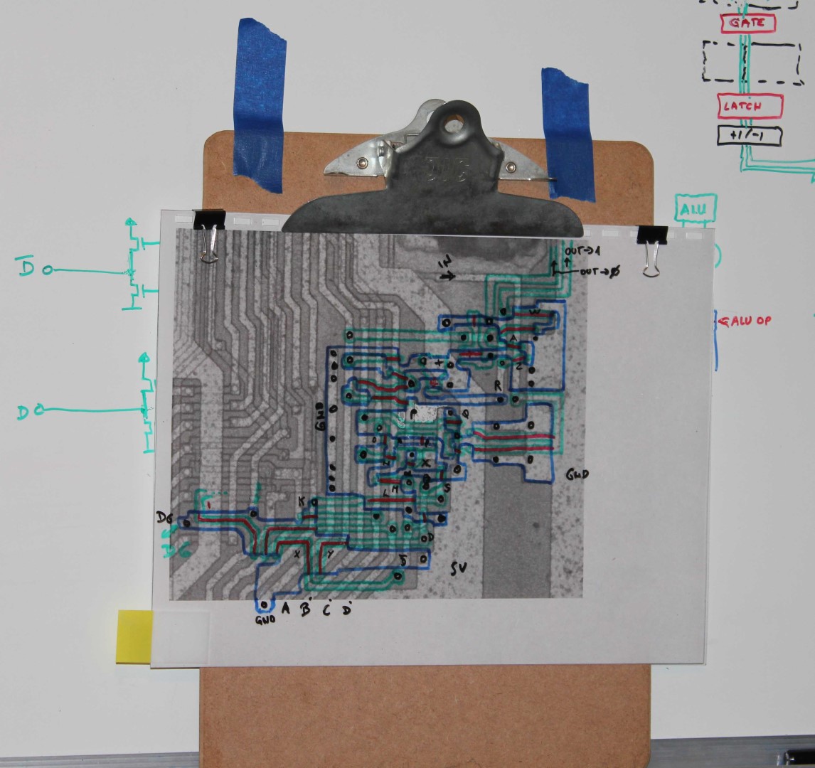
Data pins (D0-D7) carry arguably the most complex signals on the Z80 since they are both bi-directional and capable of tri-stating. They are located around the +5V pin – four of them on each side. This is a microphotograph of a gate of one of the data pins which we will look at more closely today – a pin for a data line D6.
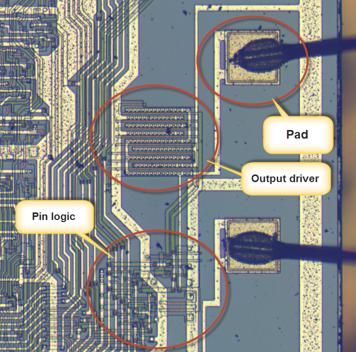
Each data pin has 3 distinct sections: a pad (to which a wire is bonded), an output driver, and the pin logic. Note that in this particular layout those sections are quite apart and there is another pad to the right of our logic which circuitry is offset below and out of the picture.
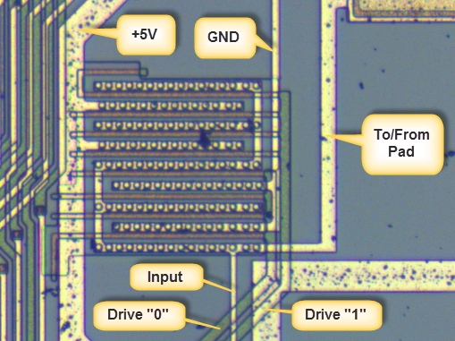
The output driver transistors are capable of directly driving the pad to either ground or 5V. See in the image below how the signals that drive logic “0” and “1” are wrapped in a comb-like structure around the ground and 5V lines. When one of those polysilicon wires is asserted (signals “1” or is being driven to a positive voltage), a transistor block (for “1”, the top half; for “0”, the bottom half) closes and passes 5V or GND through and out to the pad line.
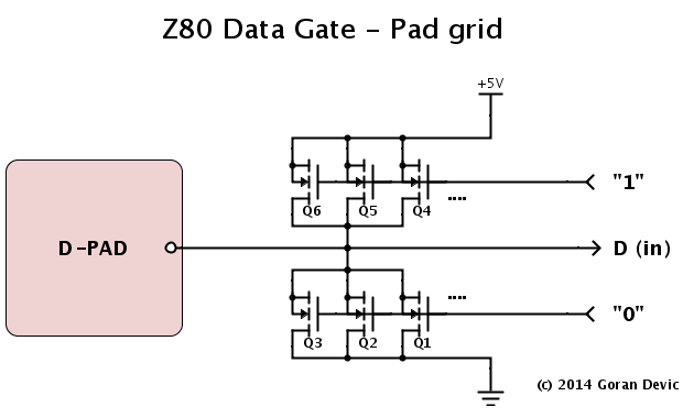
This schematic corresponds to the image: a gate is tri-stated when both “1” and “0” driver signals are not active. (They both should never be set at the same time.)
Those two comb-like sections also provide input voltage spike protection. See Zilog’s patent US4605980 that explains that aspect of the design.
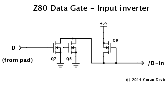
Let’s trace and follow the input wire marked as “D (in)” into the logic. We find it ends as a gate of a transistor that inverts the signal. This not only isolates it electrically from affecting the output but also improves the input signal quality by normalizing (amplifying) it.
The schematic created from the image shows more clearly how the input data bit gets inverted and also pulled up which makes it “1” when not explicitly being driven to “0” by the input signal.
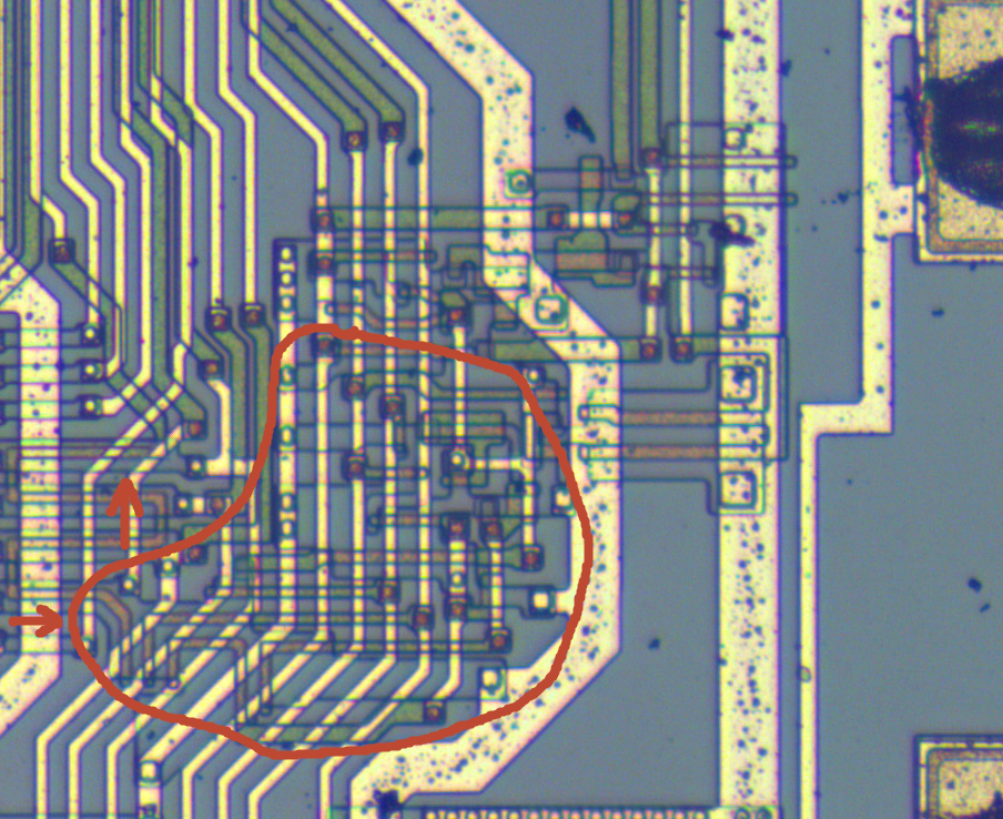
We move on and will now examine the main logic circuit implemented within this region:
Its schematic is:
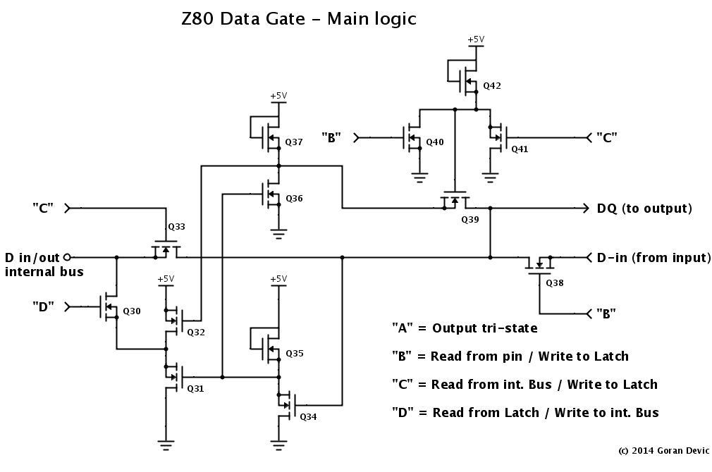
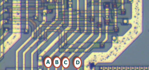
Four control signal lines run along and connect to each of the eight data gates along the chip edge. I marked them as “A”, “B”, “C” and “D”. Their function is:
- “A” when high, tri-states the output pin by grounding both (“1” and “0”) output driver signals.
- “B” when high, reads a data bit from the input pin and also writes it into the latch.
- “C” when high, writes a bit from the internal data bus out onto the data pad and also writes it into the latch.
- “D” when high, reads a bit from the latch into the internal data bus. The signal from the pad is ignored.
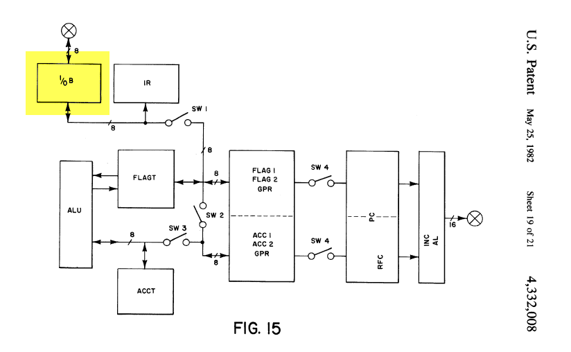
The latch provides additional temporary data storage. Since there are 8 gates in total – one for each data bit – they can be thought of as another full 8-bit register sitting on the data bus. To illustrate its usefulness, consider the instruction “LD (IX+d), n”. It loads a byte “n” and keeps it in that data latch during the computation of (IX+d). Without it, not only there would be no other place to keep it, but it would also take another T-cycle to store it somewhere and to later read it out. This additional operation would also require the use of an internal data bus which could not be used in parallel for the ALU address calculation. That latch can also be seen from a block diagram shown in a Zilog patent US4332008.
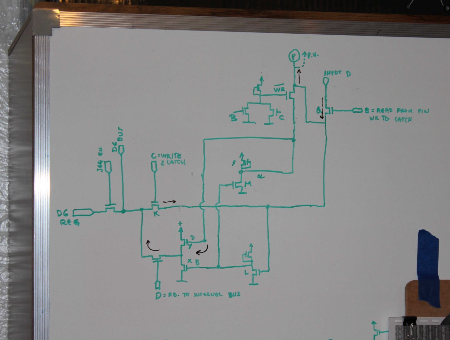
The following diagram illustrates the internal latch operation implemented with transistors Q34 (and its pull-up, Q35) and Q36 (and its pull-up, Q37).
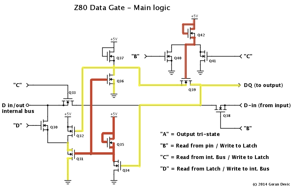
In this particular example, a “0” is being latched and kept stable by a two-inverter feedback loop. If a control signal “B” is asserted (control unit wants to read and latch a bit from the pad), Q40 saturates (closes) and drains to the ground. Q42 can’t pull it up any longer and the segment is grounded. Q39 opens and breaks the inverter-based latch loop. At the same time, Q38 closes and a bit from D-in enters the loop. It sets the Q34 to either high or low (from the input) and when “B” eventually de-asserts, that bit is latched in.
Similarly, you can follow what happens when any other control signal is asserted.
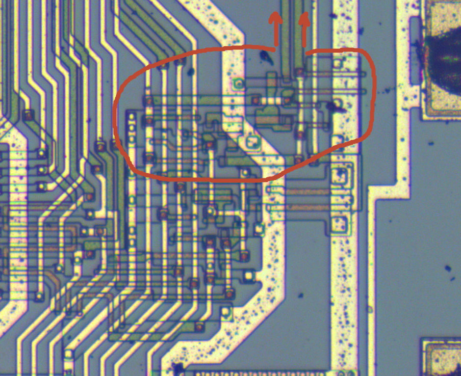
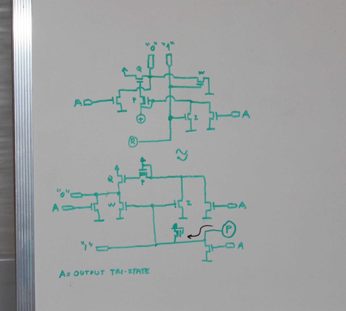
Lastly, let’s visit the output circuitry since, surprisingly, it is not trivial. It is located within this area:
And this is the schematic:
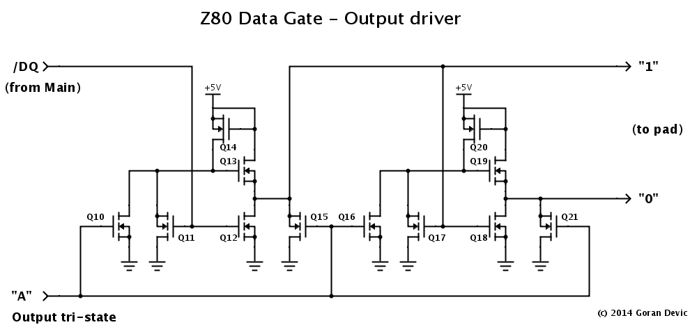
There are two nearly identical sections, one for the input bit itself and the other for its inversion (remember the output drivers need both “1” and “0” signals). Each signal is driven by a strong push-pull configuration (Q12+Q13 for the “D”-bit and Q19+Q20 for its inversion, “/D”). Q12 is the main inverter leading into the second part.
This circuit uses the control signal “A” which causes the output to be tri-stated. It does it by grounding signals at several key places.
By following a data bit from the pad and into the internal data bus, and through all the gates and inverters presented in this text, it can be shown that the internal data bus of the Z80 processor carries inverted data bits. This would effectively not matter since at every design block where data bits are used, they are inverted again. One of the uses of an NMOS inverter is to amplify the signal between endpoints of long segments. Such inverters would cancel each other when placed at the endpoints.
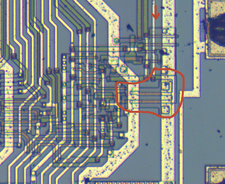
Coincidentally, the SW1 (a data bus switch) from the patent diagram image shown above can be found right in this neighborhood:
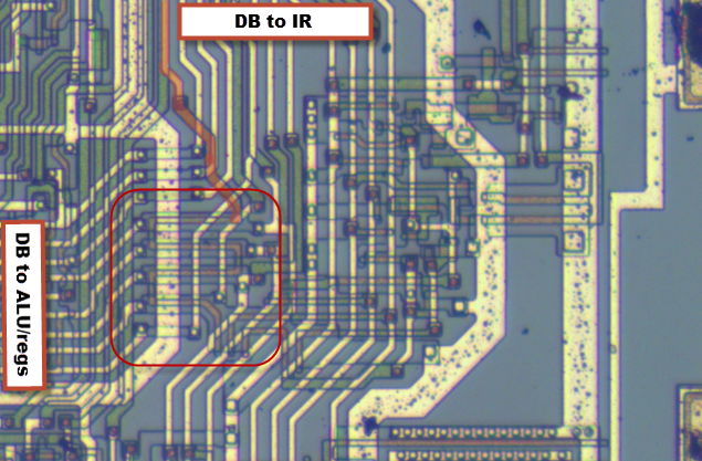
In this picture on the left edge, the internal data bus connects to the ALU and the register file. On the top, it connects to the Instruction Register latch described in this post. The SW1 is implemented using a control signal (highlighted in red) which becomes a distinct “S”-shaped polysilicon transistor gate gating 4 bits of a data bus at this location and effectively disconnecting it when the signal is low. (The other 4 bits are gated elsewhere. Hint: look close to the 5V pin!).
Reading patents can provide valuable missing information of a design.
Z80 Address Gate
Just for the curious, this is an image of one of the Z80 address gates (A15 gate, located close to the corner of a chip). Transistors are marked with red lines across the substrate (in blue) they gate. Polysilicon wires are green. Transistors forms when polysilicon wires intersect the substrate.
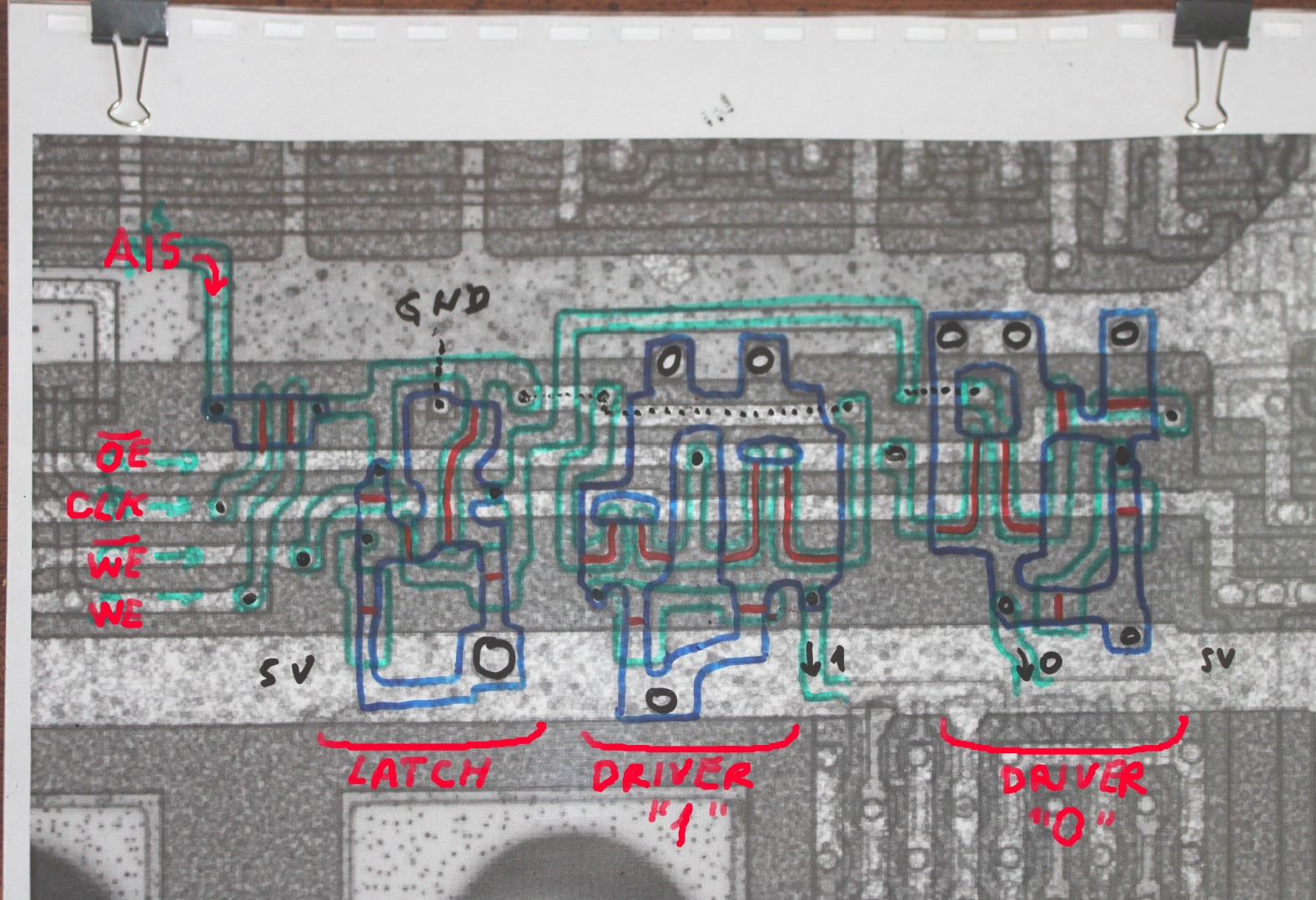
I hope that even without the schematic diagram you can now see three separate sections: the latch, formed by two inverters and two pull-ups, holds up the output value; a push-pull driver that drives the address value of “1” to the pad and a similar driver for “0”.
The latch works as a transparent latch and is also gated by the clock to limit transitions to the duration of positive clock pulses. /OE control line, when asserted, will tri-state both drivers and make the address pin assume high-Z. The bottom two control lines are “write enable” and its complement: one enables the input from its internal address bus line while its complement breaks up the loop between the two inverters so a new value can be written without the latch fighting it.
Backup images (click to enlarge):
unbelieveable !
I believe the arrangement of Q13/14 and Q19/20 form what is known as a “bootstrap load”, the purpose of which is to supply a higher-than-VCC voltage to drive the output transistor gates fully on. The purpose of the “A” input is not only to tri-state the outputs, but to “pump up” these bootstrap loads.
Hi, Goran. Fantastic article it is really good to be able to see the implementation of a device like the Z80 in detail like you have done! Congratulations!
But I believe there may be an important error in the schematics. I do not think they would be able to connect the bulk of the NMOS devices to different nodes in the circuit. They would need N-Wells & P-Wells for that, and I do not think this was the case for NMOS technologies of the time. I think all the NMOS bulks would be connected to the substrate. More like it is shown in this wikipedia diagram:
https://en.wikipedia.org/wiki/Depletion-load_NMOS_logic#/media/File:Nmos_depletion_and.svg
Supposing the process was made with “p-” wafers and drain/source with “n+” diffusions, the p- substrate would be a common net between all enhancement mosfets. Alternatively in a twin well technology which is common in latter CMOS technologies you would have an N-Well to implement the PMOS devices and then a P-WELL, shallower than the N-Well, where you could have isolated NMOS devices with the bulk (P-Well) available to connect in nets different than the substrate. In any case, that net would never be the supply, otherwise source/drain of the transistors could neve be more than a diode bellow supply.
Those wells demande large transition areas. And we would not be able to see the different transitions intermingled like we see in the Z80 layout images. Hence my comment.
Thank you for your comment, and you are most likely correct.