In the last article, I described the sequencer, which is the heart of a CPU, and a few other blocks that perform various tasks. But how is it all orchestrated to perform useful work?
Enter the PLA and the Timing matrix – the mind of a CPU.
PLA (Programmable Logic Array) statically decodes groups of instructions by matching individual bits of the opcode. The instruction register directly feeds its 8 bits into the PLA and holds its value for the duration of instruction execution. However, there are 7 more control wires going into the PLA (array). Those represent: IX/IY prefix is active (1 bit for active and 1 bit for inverse of it), not in halt bit, ALU operation bit, executing regular instruction (no prefix) bit, CB prefix is active bit and ED prefix is an active bit. They modify the result of the PLA matrix based on those states to trigger different actions.
I have used a PLA table from Ken’s blog here and created a C# program that lets us experiment with it. See the “z80_pla_checker” tool: You can run the executable and check, for example, which PLA entry triggers on which instruction and the other way around.
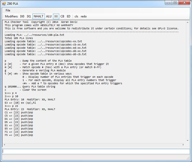
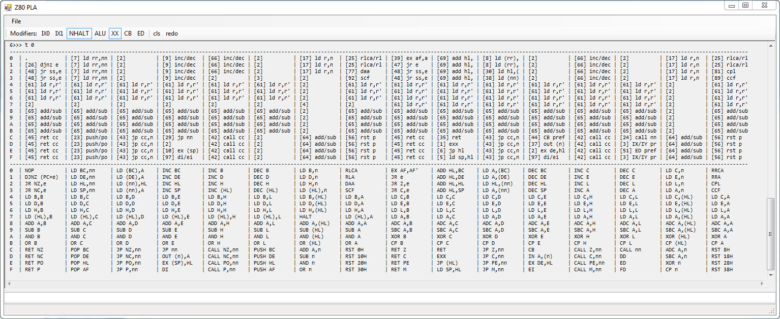
For example, the image below shows the tool dumping a complete instruction table and the corresponding PLA indices:
The tool implements those additional PLA bits and they can be toggled on and off to check their effect on the final PLA selection.
In the end, the tool dumps raw SystemVerilog code that implements the PLA in the design; the code which you can see here.
The timing matrix contains a set of operations for each statically decoded instruction (remember the PLA?) and determines which control signals fire at which M and T clock combinations as the sequencer generates them.
In its simplest form, the timing matrix says: “On M1 and T1, and when the instruction (PLA output) is such and such; activate control signals A, B and C”, that, for every instruction, M and T combinations. In software (as well as in Verilog), this translates into a pile of “if” statements. In hardware, however, CPU designs are highly optimized and these equations translate into a form of, “Fire control signal A when M1 is set and T1 is set and PLA wire 5 is set”, that, for every control signal. The “and”s in those statements become simple AND gates.
The timing matrix is contained in the “Timings.xlsm” file. This image shows a portion of it – the entries describing 8-bit ALU instruction groups:
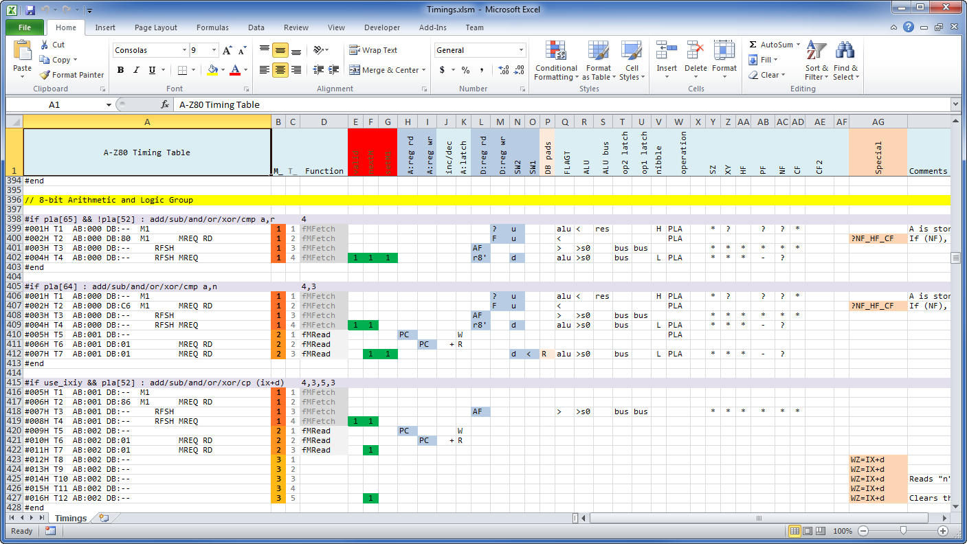
The columns represent symbolic operations on various blocks resulting in control signals emitted at precisely specified M and T clock times. There is a subtle balance implied in the organization of this file: on one hand, we could have directly specified all 100+ control signals and marked each of them active when needed, but that would be unmanageable and error-prone. On the other hand, we could have abstracted it even more in which case we lose the ability to precisely define operations.
How does this timing information get into the design?
This Excel file has a macro built-in (“Developer” / “Macro”) which exports it into a tab-delimited text file for further processing. Most of the (key) words in that file are the abstraction of and stand for one or more control signals, and the Python script “genmatrix.py” processes it while looking at the “timing_macros.i” file that contains mappings between each token and a set of control wires. In the end, it generates a Verilog include file “exec_matrix.vh” which is, frankly, hard on human eyes but Quartus loves it when compiling it into the CPU.
How did I arrive at a sequence for each instruction?
The timings on the Z80 bus are known but I still run an Arduino dongle to dump external pin response to each instruction: the tables for regular opcodes are here, those with CB prefix here, ED prefix here, DD+CB here, and DD only here. Then I correlated the functions with internal machine cycles (M) using those tables and several other sources while matching the possible operations on internal busses and blocks for each T-cycle in between.
For some instructions, I struggled quite a bit – there is nothing like spending a weekend trying to figure out a puzzle of how a Z80 would implement an instruction – for example, RLD or RRD, as shown on my kitchen counter here:
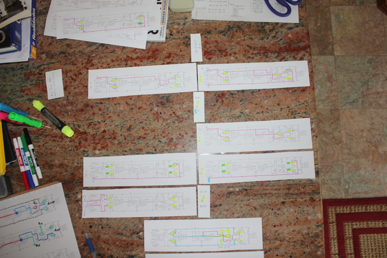
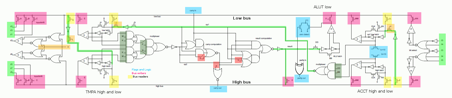
These two in particular were hairy: the ALU has only certain paths and control signals. Those need to be used to perform an operation. Since the ALU is based on Ken’s reverse-engineered blueprint, that’s what I had to work with:
For other instructions, I assumed the Z80 was extremely optimized and had different blocks operate on their own to minimize inter-dependency and the problems they could cause, so I was looking into as much regularity and a certain “beat” and beauty of the timings. That’s hard to explain in words, but you know it when it feels right.
In the end (and this is now a big leap in this text), a ModelSim simulation shows how it all works together:
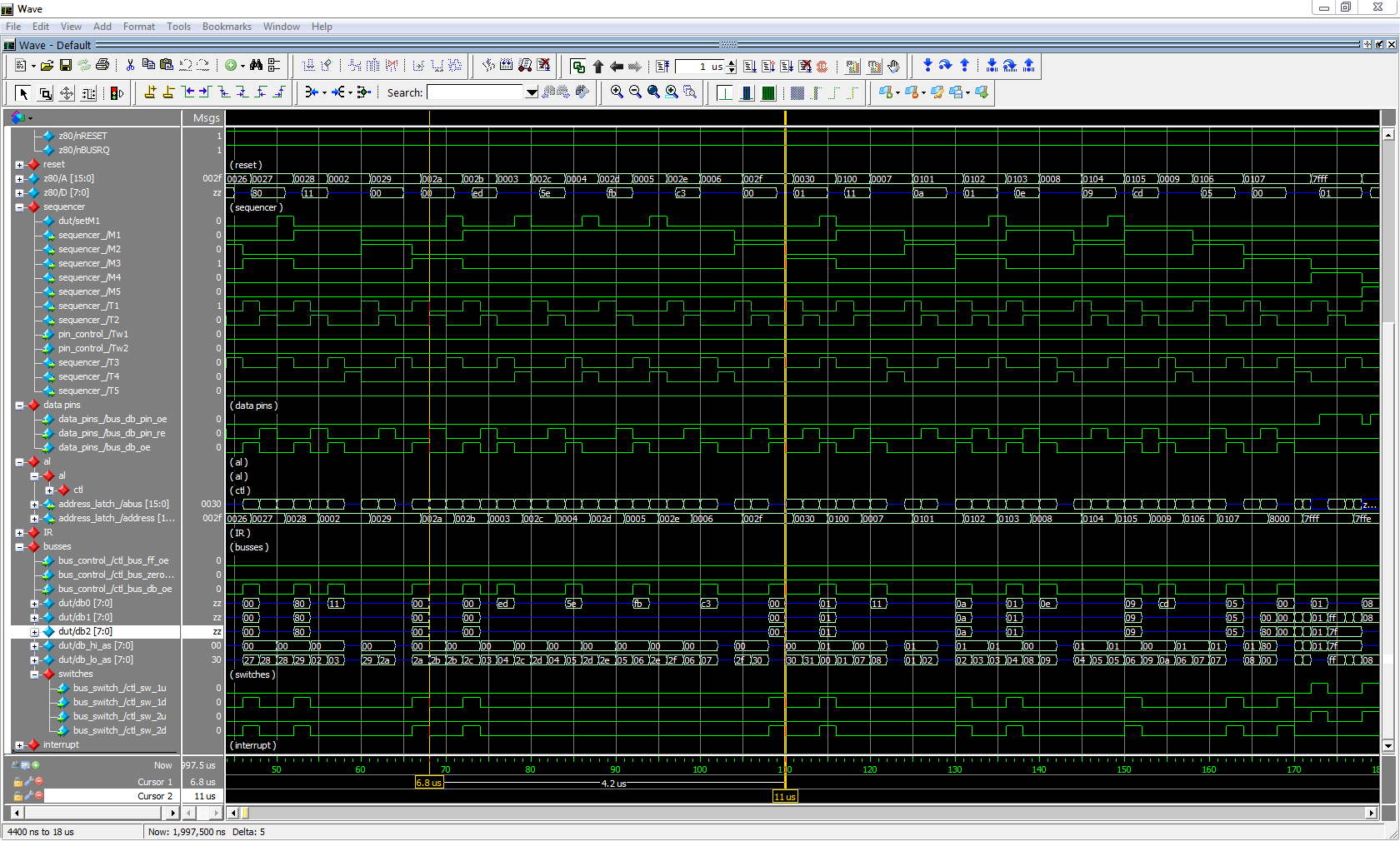
Once the sequencer is unleashed – and you can see its M and T cycles on the image, various control signals are activated at pre-determined times and the CPU keeps chugging along.
The key to a working design is to keep simulating and testing at every step.
I have used a set of Fuse tests. Fuse is one of many Z80 software emulators. It, however, contains a nice set of raw instruction test vectors and they include discrete start and end conditions as well as operations on memory and IO. You can see Fuse tests in “cpu\toplevel\fuse”. A script “genfuse.py” generates a SystemVerilog test file for any number of selected Z80 instructions. That mechanism allowed me to keep re-checking opcode behavior and, ultimately, to get a design that just worked.
[…] The Mind […]