If you want to find out exactly what a venerable Z80 is doing on its bus while executing instructions, in this post I outlined a dongle and the software that will let you see that. Using just a few components and connecting them to an Arduino Mega, you can trace instructions clock by clock and observe what’s happening on the bus.
Start with a proto-board and solder down components following this schematics:
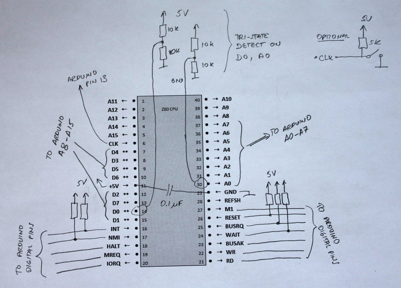
There is a capacitor between +5V and GND which should help keep away any voltage noise. You can use anything: I had a 0.1uF tantalum cap that I used. The evil thing with not putting bypass (or decoupling) caps in your designs is that you may never find out why they might behave erratically.
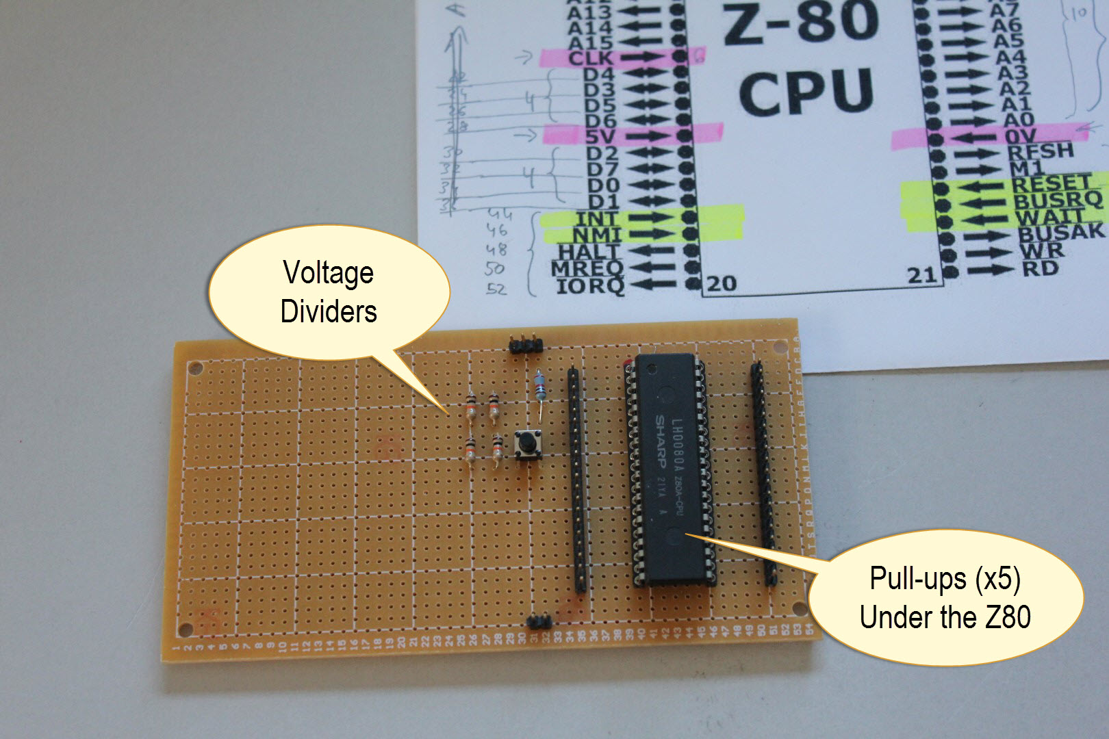
There is also a push-button, which is optional. You might think it would be connected to the reset pin but it is connected to the CLK – I wanted to be able to manually clock the Z80 to see if it worked before hooking it up to Arduino. For the same reason, every Z80 control input pin has a weak pull-up resistor. That should make it “alive and kicking” right off the bat without the need for anything else externally driving it.
Now, the most interesting extension to the design is a tri-state bus detection. Z80 occasionally puts its address and data buses into “High-Z”, or tri-state, and I wanted to detect that (it also lets most of its control pins to Z, but I was content to detect only the major buses.) There are 2+2 resistors (each 10K) making up a weak resistor divider network connected to pins D0 and A0. That way, whenever Z80 releases its data or address bus, the pins will assume 2.5V pulled by resistor dividers. Since both buses are connected to analog input pins, Arduino will be able to read the voltage and clearly detect that they are not 0V or 5V (logical 0 or 1) but somewhere in between.
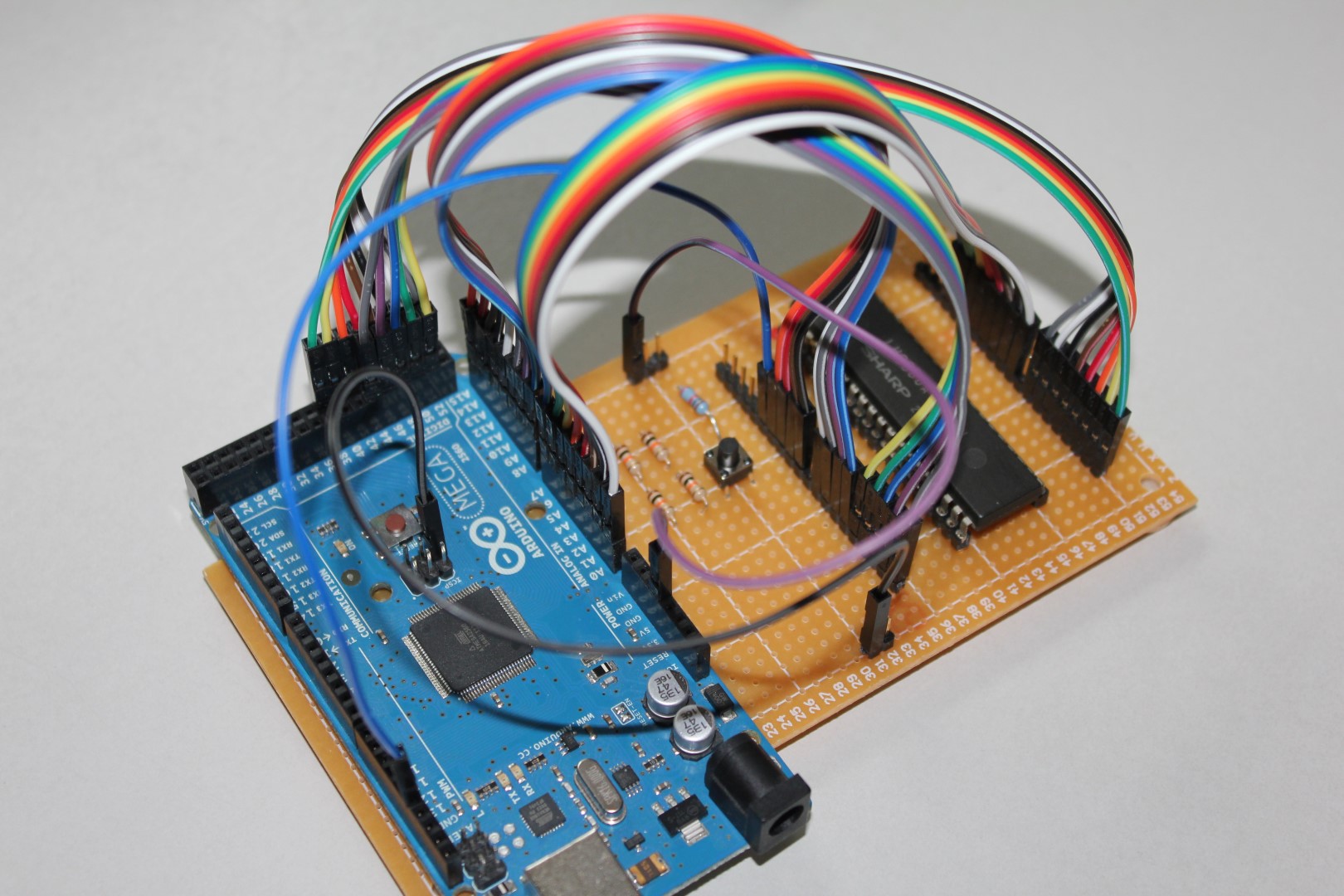
After verifying that my 25-year old Z80 chip from my parts bin is still working (!), I connected it to an Arduino Mega board. Mega is really useful here since it hosts more I/O pins than you’d ever need, runs on +5V, and therefore needs no voltage level translators to talk to Z80.
The connectors are conveniently clustered by their function: All eight data wires together, address wires (I only used 8 for a max address space of 256 bytes), control signals in two groups (one from each side of the Z80 package), and a few odd ones: clock, which goes to pin 13 on Arduino and also powers the LED on it, and +5V and GND. You can click on an image below to zoom on it —
The time is to write some software. Being a software engineer by trade comes in really useful since many great hardware hobbyists totally drop the ball when it’s time to blow a breath of life into their designs and write code, so they skim over that part. The Arduino software that runs this dongle can be downloaded here.
Connected through a serial port, you have several commands available (type “?” or “h” at the console):
s            - show simulation variables
s #var value - set simulation variable number to a value
sc           - clear simulation variables to their default values
r            - restart the simulation
:INTEL-HEX   - reload RAM buffer with a given data stream
m            - dump the content of the RAM buffer
mc           - clear the RAM buffer
There are several internal simulation variables that you can change in order to run your tests on Z80 in various ways. The best way to create a Z80 test is to download a Z80 assembler such as zmac and create a small test program. For example, create a test like this:
start:
    ei
    im 2
    ld ix, 80h
    srl (ix+20h),b
    adc hl, de
    ld hl, 30h
    ld de, 40h
    ld bc, 3h
    ldir
    ld bc, 1
    ldir
    halt
    org 38h
    ei
    reti
    org 66h
    ei
    reti
end
Functionally, this sequence does not make much sense, but it lets us test several things: Instruction prefix IX, undocumented opcode, LDIR loop, HALT; then by inserting an NMI and INT at certain places we can trace what’s going on when the CPU is servicing those interrupts.
Assemble it and zmac will generate several output files. Open an Intel-style hex file that will show the code in hex; copy all and paste it into the Arduino serial terminal.
:10000000FBED5EDD218000DDCB2038ED5A21300094
:0E001000114000010300EDB0010100EDB076DB
:03003800FBED4D90
:03006600FBED4D62
:0000000000
Arduino will happily respond that it stored the stream of bytes and you can issue a command “m” to dump the buffer (which Z80 sees as its RAM) to confirm that it is there:
    00 01 02 03 04 05 06 07 08 09 0A 0B 0C 0D 0E 0F
   +-----------------------------------------------
00 |FB ED 5E DD 21 80 00 DD CB 20 38 ED 5A 21 30 00
01 |11 40 00 01 03 00 ED B0 01 01 00 ED B0 76 00 00
02 |00 00 00 00 00 00 00 00 00 00 00 00 00 00 00 00
03 |00 00 00 00 00 00 00 00 FB ED 4D 00 00 00 00 00
04 |00 00 00 00 00 00 00 00 00 00 00 00 00 00 00 00
05 |00 00 00 00 00 00 00 00 00 00 00 00 00 00 00 00
06 |00 00 00 00 00 00 FB ED 4D 00 00 00 00 00 00 00
07 |00 00 00 00 00 00 00 00 00 00 00 00 00 00 00 00
08 |00 00 00 00 00 00 00 00 00 00 00 00 00 00 00 00
09 |00 00 00 00 00 00 00 00 00 00 00 00 00 00 00 00
0A |00 00 00 00 00 00 00 00 00 00 00 00 00 00 00 00
0B |00 00 00 00 00 00 00 00 00 00 00 00 00 00 00 00
0C |00 00 00 00 00 00 00 00 00 00 00 00 00 00 00 00
0D |00 00 00 00 00 00 00 00 00 00 00 00 00 00 00 00
0E |00 00 00 00 00 00 00 00 00 00 00 00 00 00 00 00
0F |00 00 00 00 00 00 00 00 00 00 00 00 00 00 00 00
Typing command “s” will show simulation variables that are available to us:
------ Simulation variables ------
#0 Trace both clock phases = 0
#1 Trace refresh cycles = 1
#2 Pause for keypress every = -1
#3 Stop after clock # = 40
#4 Stop after # M1 cycles = -1
#5 Stop at HALT = 1
#6 Issue INT at clock # = -1
#7 Issue NMI at clock # = -1
#8 Issue BUSRQ at clock # = -1
#9 Issue RESET at clock # = -1
#10 Issue WAIT at clock # = -1
#11 Clear all at clock # = -1
#12 Push IORQ vector #(hex) = FF
The code evolved over time and so did the variables and multitudes of situations that can be set up by cleverly combining those values. In fact, this blog probably does not show the most up-to-date software version.
As it runs, the trace program counts clocks and, by setting those variables, you can toggle specific control pins at determined times. For example, if you want to issue an NMI at clock 20, you would do “s 6 20”. You can optionally dump what’s happening on both clock phases and not only on the positive phase (variable #0). Variable #1 will show or hide memory refresh cycles that accompany M1.
Start the trace by issuing a command “r”. The Arduino starts the clocks and issues a RESET sequence to Z80 after which your code runs and bus values are dumped out.
Notice the tri-state detection – when the address or data bus is being tri-stated by Z80, the program outputs “–“. In fact, the data bus is being tri-stated most of the time! This is a dump from the start of the run. The dumps are normally longer, but you get the idea.
Performing a RESET
Starting the clock
-----------------------------------------------------------+
#001H T1 AB:--- DB:-- RD                                   |
#002H T2 AB:--- DB:--                                      |
-----------------------------------------------------------+
#003H T1 AB:000 DB:-- M1                                   |
#004H T2 AB:000 DB:FB M1 MREQ RD      Opcode read from 000 -> FB
#005H T3 AB:000 DB:-- RFSH                                 |
#006H T4 AB:000 DB:-- RFSH MREQ       Refresh address 000  |
-----------------------------------------------------------+
#007H T1 AB:001 DB:-- M1                                   |
#008H T2 AB:001 DB:ED M1 MREQ RD      Opcode read from 001 -> ED
#009H T3 AB:001 DB:-- RFSH                                 |
#010H T4 AB:001 DB:-- RFSH MREQ       Refresh address 001  |
-----------------------------------------------------------+
Immediately we can see that Z80 uses 2 clocks of not doing anything externally after the reset. The clock phase can be high (H) or low (L) and dumping lows is enabled by setting a simulation variable #0 (by default, it does not dump low phases). T-cycles are being automatically counted starting at every M1 cycle. This greatly helps to cross-check each instruction against documentation. Input and output pins that are active are also tagged.
The Arduino simulator software provides data bytes to Z80 on memory read operations and stores bytes into the internal buffer on memory write operations. Simulating an IO map is much simpler where variable #12 can be used to push an arbitrary IORQ vector when needed.
Overall, the dongle itself and the options implemented by the Arduino software provide a powerful way to examine and visualize Z80 behavior whether it is running undocumented opcodes or responding to a sequence of external control pins like interrupts, bus requests, etc.
If you’ve found this interesting, you may want to check my other post where I documented some of the Z80 behavior which I’ve found less known.
This is great! How much feedback have you gotten? I registered but didn’t get an activation email.
I was getting too much spam, so I tightened up the filters on the blog sites, Mikhail. People mostly email me and we have email conversations.
Hi,
I’m trying to do a similar thing: I’m connecting a Z80 to a Teensy (an Arduino mega compatible), which in turn is connected to the same SRAM wired to the Z80, and to an SD card interface.
The idea is to use DMA (BUSRQ low) in order to load into SRAM a boot file, and subsequently start the Z80 via a RESET.
My problem is that I cannot manage to put the BUSRQ pin LOW (this pin is connected to a digital I/O pin on the Arduino): I’ve noticed that in your schematics you’ve put pull-up resistor on each Z80 input pin, but that those resistor does not appear in the photos of your final project.
Should I also put them on my Z80 inputs, in order to making those pin to ground, by writing a LOW value on the connected Arduino pins ?
Thanks in advance for any help.
Hi,
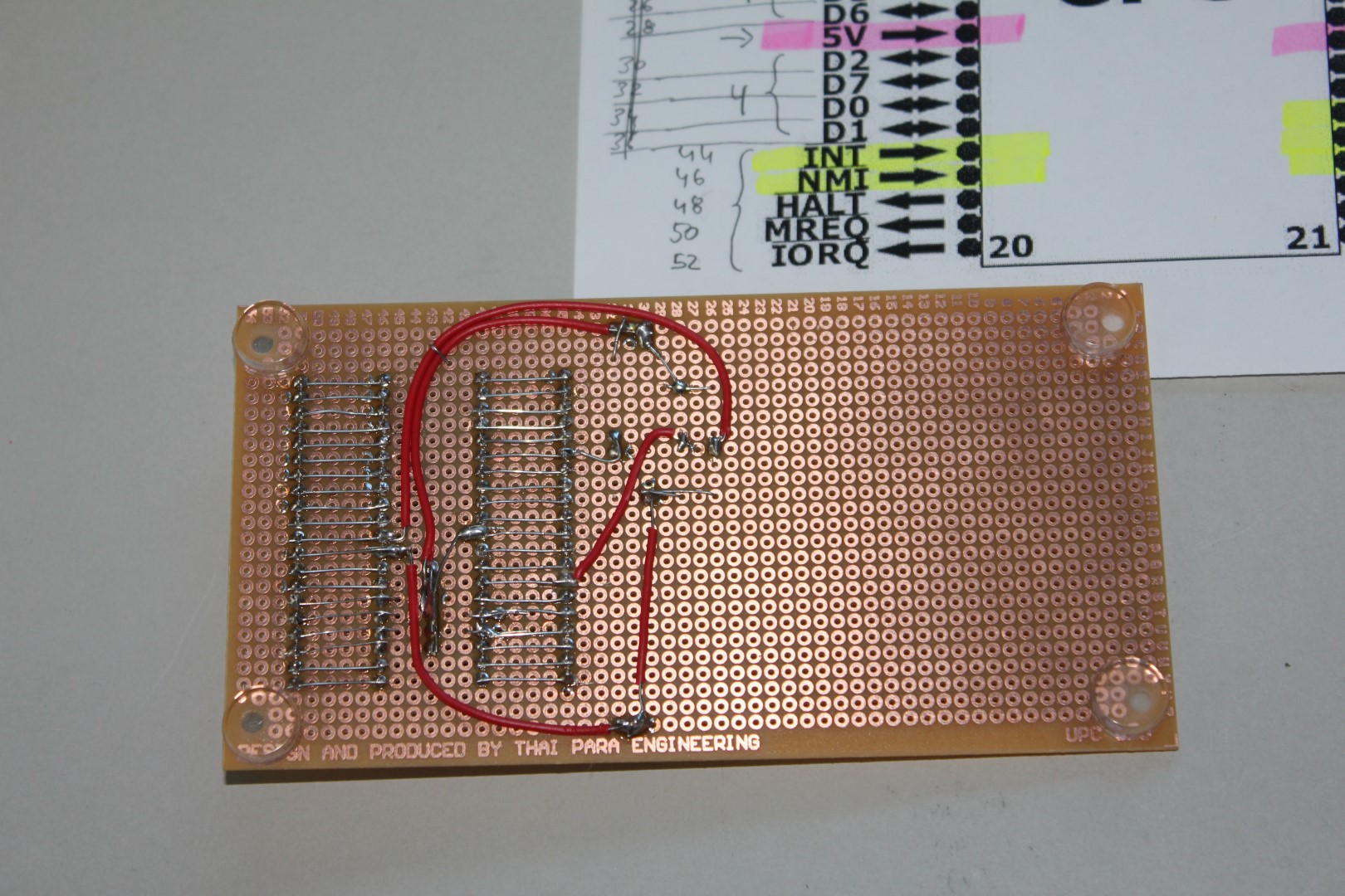
Thank you for your note – I have corrected the image to indicate that the other 5 pull-ups are actually located under the Z80 and cannot be seen.
I have added weak pull-ups to be able to power up the board without having the Arduino attached. Then I can clock it manually using the push-button and check that Z80 is not dead. That definitely gets one variable out of the way. Although pull-ups are probably not needed once you have other means of driving the inputs, they would not hurt. In fact, they’d keep Z80 stable until your Arduino initializes its IO pins.
Note that the pull-ups are connected to +5V since the Z80 uses inverted logic. You’d drive BUSRQ to ground, but then you have to wait until BUSACQ responds – see the Z80 manual and “Bus Request/Ack Cycle” timings. For BUSACQ to respond, it needs a stable clock for at least 2T (bus req latch in + ack change state), which means the CPU has initialized (run the RESET sequence). Your scheme might be much more involved than simply power up with BUSRQ low. Z80 behavior is very erratic until properly reset, so try to issue a reset first (make sure the CLK is also clocking the Z80), hold reset low for a minimum of 3 full clock cycles, release reset and assert BUSRQ (to ground), wait until Z80 drops BUSACK to 0 and then all busses should be in high-Z and available for Arduino to access the SRAM. Also, MREQ, IORQ, RD and WR should be available (not all Z80 control pins go to high impedance!)
Good luck and tell me how it goes!
Thanks Goran !
I’ll keep you informed 🙂
I’ll put the pullup resistors, and I’ll try to reset the Z80 before asserting BUSRQ to LOW (I’m running it at 8MHz, clocking it directly from the Arduino).
Another question if I may: when the busses goes in high-Z, also the MREQ, IORQ, RD and WR control pin go high-Z right ?
Thanks again.
Yes, (only) those 4 control pins go high-Z. That should be sufficient for a device external to Z80 to access memory (notice the MRFSH is not on that list which could be a problem for dynamic RAMs if the BUSRQ is held low for too long. Not your case.)
I am not quite sure – and it will be interesting to find out the exact sequence – if the Z80 will try to fetch/execute an instruction at address 0 first before latching the BUSRQ, so you might see an initial M1 read and the BUSRQ will be accepted at T=4. See the timing diagrams for BUSRQ. That means you really need to poll for BUSACK and it may take a few extra clocks.
I would suggest not running at 8 MHz at first but toggling it tick by tick until you get things running, and then gradually crank up the frequency. Depending on your wires and connections, you might get too much noise on the lines to get it stable at 8. If you have an oscilloscope or a logic analyzer, you might be able to get a better feel on when the noise becomes an issue.
Hi Goran,
I’ve finally managed to to boot the Z80 from the Teensy.
The Teensy lowers the BUSREQ pin, isolate the Z80 from the circuit, loads an assembler binary to SRAM from an SD Card, and then resets the Z80.
See this in action:
http://youtu.be/IKXadt095pw?list=UUWfak0EEvdF6QQyG5_UtbCA
I’m now trying to use the Teensy serial as a Z80 peripheral, but the Teensy is too slow to respond to the Z80 queries.
I’m thinking to use the WAIT pin in order to freeze the Z80 temporarily, in order to allow the Teensy to correctly get data from the Z80.
Hello Goran,
The work you did here to annotate the machine cycles and T-states of all Z80 instructions was invaluable to me for my own Z80 emulator. Unlike most Z80 ‘functional’ emulators, mine attempts to faithfully reproduce all of the Z80’s timing states, meaning my emulator should produce the exact same captured M-cycle and T-state results as your Z80/Arduino project did for all Z80 instructions.
I was especially impressed with your method for determining when the data and/or address lines were in a high-impedance state. Very nice!
I was a bit disappointed that your published results only listed the captured clock high states within each clock cycle, so I couldn’t tell exactly when a control status line changed state. For example, for standard M1 opcode fetch cycles, your results always show the /M1 status line active/low at T1, and the /MREQ and /RD status lines active/low at T2. But those results are a bit misleading: in fact all of those status lines are activated during T1 — the /M1 status line is activated at T1 high, while the /MREQ and /RD status lines are activated at T1 low. If your results listed both the clock high and clock low states (a nicely designed option in your Arduino sketch), then I would be able to see exactly when those status lines changed state.
I really enjoyed your commentary on ‘unusual’ Z80 behaviors, especially your comments re the initial state of the Z80’s registers and flags following power-on/reset. I performed similar experiments to yours and my results were ‘almost’ identical to yours. Like you, I confirmed that all registers other than PC and IR — as documented, reset always clears PC and IR — have all their bits set (0xFF or 0xFFFF), except for the F (flags) register. In my case the F register was initialized differently than yours. After executing a PUSH AF instruction immediately following power-on/reset, I determined the value of the F register by examining the data lines during the instruction’s second memory write cycle. That value was 0x6C, not 0xFD as your results indicated. 0x6C is a pretty weird value: flags Z, P/V and the undocumented X and Y flags are set; flags S, H, N and C are reset). I don’t which type of Z80 chip you were using for your experiments, maybe the NMOS and CMOS versions behave differently in this respect.
Speaking of NMOS and CMOS versions: One problem I ran into doing my experiments was that single-stepping the Z80’s clock or running the clock at very slow speeds worked fine on my CMOS Z80 chip, but produced incorrect results on the two NMOS chips I tried. For example, when I tried testing the instruction ‘JR e’ on an NMOS chip connected to a 1 Hz clock, the PC value following the instruction was incorrect, but was correct when I replaced the NMOS chip with a CMOS version. (And yes, I scoped the clock line and confirmed that the clock signal was clean, with fast rise and fall times.) I finally figured out why when I looked more carefully at the Z80’s specs. The NMOS Z80 specs lists the maximum clock pulse low width and clock pulse high width as 2000 nsecs (2 usecs). For a clock with a 50% duty cycle, that translates to a minimum clock speed of 250 KHz. The CMOS Z80 specs list the maximum clock pulse low width and clock pulse high width as ‘DC’, meaning the CLK line can be held in a high or low state for an indefinite period. The moral of this story: if you’re trying to capture Z80 state by single-stepping the clock or running it at very low frequencies, be sure to use a CMOS version of the Z80 chip; otherwise you might get bad results.
I’ll add a new reply to comment on the results of your other Z80 experiments.
Thanks again for your fascinating and valuable work on the Z80’s undocumented behaviors!
Here’s my second post to comment on your excellent findings re undocumented Z80 behaviors. I’m referring to your commentary on http://www.baltazarstudios.com/files/Z80-undocumented-behavior.htm.
1. RESET
As I mentioned in my last reply, my findings matched yours exactly except for the initial state of the F register following a power-on/reset. You found the F register’s value to be 0xFD (all but the C flag set); I found F’s value to 0x6C. I just reran that experiment, using the exact same hardware as before, and this time the F register’s value was 0x44 (Z flag (bit 6) and undocumented X flag (bit 3) set, all others reset). Not sure why the different result, as I was consistently getting 0x6C before. I’ll continue investigating.
——————————————————————————————————–
2. Register values after the RESET
My results match yours exactly.
——————————————————————————————————–
3. RST
You mentioned, ‘see the extra 2 (clock cycles) before pushing the PC.’ Actually, there’s only one. Zilog documents the RST instruction as requiring a 5 T-state M1 (opcode fetch) cycle, followed by two 3 T-state MWrite cycles; a total of 11 T-states. In your listing, which also shows a total of 11 T-states, T6 is the first T-state of the first MWrite cycle and T9 is the first T-state start of the second MWrite cycle. Since your listing only shows status when the clock is high, there’s is no visible difference between T5 and T6. Had you listed the clock low states as well, you would have seen the /MREQ line activated at T6 low (and T9 low), indicating the start of a new MRead or MWrite cycle (in this case an MWrite cycle).
——————————————————————————————————–
4. PUSH BC, see how the 5-3-3 clocks are distributed
No surprises here; exactly as documented.
——————————————————————————————————–
5. PUSH IX just adds another 4-cycle prefix to it
Again no surprises.
——————————————————————————————————–
6. This is a difference between 2 cycles of LDIR …
The reason for the 5 extra T-states when B 0 is that the Z80 needs to execute an ALU cycle to decrement the PC by 2 (to repeat the same LDIR instruction). It has to ‘burn cycles’ to do that since it can’t overlap the decrement operation with the next instruction.
When BC = 0, the PC is already pointing to the next instruction, so that M-cycle is not needed.
——————————————————————————————————–
7. ADD HL,ss seems to have too many cycles …
Zilog documents this instruction T-states as 11 (4, 3, 3). As your listing shows, the first four T-states is the M1 opcode fetch cycle. No status lines are active for the next 7 T-states. These are separate ALU cycles needed to add the ss register’s lsb to register L and the ss register’s msb to register H. In my research the shortest ALU cycles is 3 T-states; the longest is 5 T-states.
It appears that, during an ALU cycle, the address lines contain the PC’s current value and the data lines are in a high-impedance state, although I haven’t confirmed this in all cases.
——————————————————————————————————–
8. This is an undocumented opcode sequence:
ld ix, 80h
srl (ix+20h),b
There’s a lot to comment on here! The SRL (IX+20h) instruction is one of the Z80’s ‘double prefix’ instructions, 4-byte instructions that begin with the prefix pair DDCB or FDCB. What makes these ‘(IX+d)’ and ‘(IY+d)’ instructions so interesting is the order of the four bytes: the two prefix bytes, followed by a d displacement operand, followed by the instruction’s main opcode. The d displacement operand occurs *before* the main opcode(!). Furthermore, as your listing confirms, while M1 cycles are used to read the two prefix bytes, an M1 cycle is *not* used to read the main opcode; instead a standard memory read cycle is used. What that means is that this class of instructions generates only *two* refresh cycles while executing (the R register is only incremented twice), since only the prefix bytes, not the main opcode, is read using an M1 cycle.
In terms of these instructions’ documented T-states — 23 (4, 4, 3, 5, 4, 3) — here’s the M-cycle sequence:
1st M-cycle (4 T-states):
M1 cycle to read the DD prefix.
2nd M-cycle (4 T-states):
M1 cycle to read the CB prefix.
3rd M-cycle (3 T-states):
MRead cycle to read the d displacement operand (20H).
4th M-cycle (5 T-states):
MRead cycle to read the main opcode (38H) and calculate IX+20H.
5th M-cycle (4 T-states):
MRead cycle to read (IX+20H) and perform the shift.
6th M-cycle (3 T-states):
MWrite cycle to write the result to (IX+20H).
Your example uses the undocumented instruction ‘srl (IX+20h),b’, which writes the shift operation’s result to both (IX+20h) *and* register B. But the sequence of machine cycles and T-states for ‘SRL (IX+d),r’ is identical to that for the documented instruction, ‘SRL (IX+d)’, so the above squence would apply to both.
——————————————————————————————————–
9. This is what happens when interrupt hits in interrupt mode 2
This one was particularly interesting to me as I hadn’t tested it myself. I was surprised by two of your findings:
1) The Interrupt Acknowledge (INTAck) cycle is 7 T-states long, including the two automatically inserted wait states (T2 and T3 in your listing). My emulator incorrectly generates only 6 T-states for the INTAck cycle, not 7.
2) The PC is pushed onto the stack (two 3 T-state MWrite cycles) *before* the interrupt service Routine (ISR) address is read from the in-memory interrupt table (two 3 T-state MRead cycles). My emulator incorrectly performs the MRead cycles *before* the MWrite cycles.
It’s a bit difficult to determine in your listing where one M-cycle ends and the next one begins because you only list the active status lines when the clock is high; it would be easier to find those splits if you showed both the clock high and clock low states.
And I certainly agree that Zilog’s documentation is lacking here and virtually everywhere else in clarifying what’s going on during each M-cycle and T-state in response to an instruction or interrupt. Zilog’S CPU User Manual’s Interrupt Mode 2 Response description (page 25-26) does offer a general idea of what happens, but your analysis certainly helps fill in the missing details. Based on your results, here’s the 19 T-state, 5 M-cycle sequence for a Mode 2 interrupt response:
1st M-cycle (7 T-states):
INTAck cycle to get the in-memory interrupt table’s offset from the
interrupting device. The address is formed by combining the I register
(MSB) and offset (LSB). Note that T2 and T3 of this cycle are automatically
inserted wait states;
2nd M-cycle (3 T-states):
MWrite cycle to push the MSB of the PC onto the stack.
3rd M-cycle (3 T-states):
MWrite cycle to push the LSB of PC onto the stack and load the PC with
the ISP address.
4th M-cycle (3 T-states):
MRead cycle to read the lsb of the Interrupt service routine (ISR)
address from the interrupt table and assign it to the PC lsb.
5th M-cycle (3 T-states):
MRead cycle to read the msb of the ISR address from the interrupt table
and assign it to the PC msb.
——————————————————————————————————–
10. This is what happens when NMI hits …
This is pretty much as documented, except, according to your listing, the M1 cycle executed in response to the NMI is 5 T-states long, not 4. This actually contradicts Zilog’s Z80 CPU User Manual (page 18), which shows T1 following T4 (not T5) in the Figure 10 timing diagram.
The two cycles used to push the PC onto the stack appear to be standard 3 T-state MWrite cycles.
I’ll test this myself to confirm your results.
Thanks again for your great work!
Hello Goran,
I’m trying to wire up this project myself and I’m wondering what you meant by 5v and GND. From your picture it looks like you are using the GND pin under the ICSP, is this true? Also are you using the 5v pin above the ground, on arduino because it looks like you are using another GND pin from the picture.
Hi Ryan,
Yes, I used GND and +Vcc from wherever I could fish them on Arduino: one GND connects to the ICSP GND pin only because I just happen to use that jumper wire (F-F). All grounds should be connected, so you can use any other GND pin. There were no other reasons.
There are only a few rules (correct power + 3-state sensing to connect to analog inputs), the rest you can connect any way you want to. For example, I had those ribbon cables which I wanted to keep together and not split them and hence this particular layout. Yours may be different; if you implement more address lines, you could probably run something more substantial than what fits in 256 bytes. Arduino RAM would be the limit.
Watch for jumper cable connections! I found that’s the weakest point as, depending on the angle they were bent and forced, the connection would be flaky. If I’d ever do this again, I’d build an Arduino shield-type of board instead just to solve that problem.
Good luck!
Hi Goran , thanks for the quick reply. I looked at the pictures more closely and figured it out. I’m currently fully connected and have the software uploaded and am getting this output (http://imgur.com/ou30UNh) to the serial monitor.
The commands that are coded in, are those to be used in the serial monitor? I’m not getting any response when hitting the commands.
Thanks again for your time.
That looks good – you got it running! The address bus is incrementing and reading NOPs.
To get the rest of it going, can you pls email me at gdevic at yahoo dot com, the response will be faster since I don’t have to log in to approve each comment. You are almost there! 🙂
[…] Today I found out a lot of projects based on Arduino and Z80, for instance this “simple” project show you how to interface a basic Arduino Mega and a Z80 […]
I have a question concerning the clock pulse.
I see you use a push button to create a single clock pulse.
I have seen some other circuits where they use a debouncing circuit in these cases. Did you experience any problems with your method?
That is a good point, John. I used that single pulse button only a few times, just to check if the Z80 is alive. Most of my work with it was through Arduino. I am sure the button would have to be debounced for a reliable operation.
Hi Goran,
This is great stuff and an excellent learning tool. Thanks for putting this together and sharing.
Why not connect all 16 Address pins to the Arduino?
Yes, you can do that, and gain control over the complete address space. If I were to do it again, I’d probably just build a custom board and have everything connected, just as you said. My board was a total hack and I did not want to solder more connections and have more dangling wires than I needed. 256 bytes was all I needed for these experiments.
When I saw the effort put into the schematic I bailed.
LoL
Hi Goran,
I seem to recall that you or someone else published a list showing the state of the Z80’s address bus, data bus and all status signals for every Z80 instruction. I thought I had a copy of that list, but can’t find it now.
If you have any recollection of this list, or know where I can find it, please let me know.
Thanks as always for your great work on the Z80.
Paul
Hi Paul, maybe you were thinking about this page? https://baltazarstudios.com/zilog-z80-undocumented-behavior/
Thank you and best regards!
Got a question for you. I found your code and liked the idea of it. I have been playing with a very simple Z80 implementation of just the Z80 and RAM + ROM. I found a very basic monitor code to use. But I thought I would like to verify it works before burning it to ROM. Thus your code is proving helpful. Problem I am seeing is I get two MREQ reads/writes for every instruction. And the same for IO reads/writes. Which messes up my attempt to try to kludge output to the 16×4 LCD. Yes, it’s a kludge but it loses the first few input characters. I tried it with your original code and loaded the first chunk of hex data in and it still does this. I can’t see how this should be possible. Maybe it’s a weird timing issue with my setup or my Z80 has an issue.
Isn’t that a refresh cycle, Tim? Every memory access will have it; RFSH pin will be asserted (active low).
Let me provide a sample as it’s easier to see what I mean. No it’s not the refresh cycle as I have that hidden as I don’t need it. Notice lines 971 and 972 (two the same MREQ RD) and 998-1000 (3 same IORQ RD). I am a retired programmer but don’t see any code error that could cause this. There are only two place this is dumped and the 2nd is not being used (as I am not showing both phases). I had increased the memory size to 4k and added the extra address lines. And removed the mask of only the low address bits. The code runs fine but the kludge I tried for input of a command depends on there only being one of these IORQ RD per instruction. But I think I see the issue from looking back at the Z80 timing diagrams. So I don’t think there is much I can do. You code does show my tiny monitor works and that is the main thing I want. I thank you for that and tip my hat to you.
#963H T2 AB:06E DB:0C M1 MREQ RD | Opcode read from 06E -> 0C-----------------------------------------------------------+
#966H T1 AB:06F DB:-- M1 |
#967H T2 AB:06F DB:3E M1 MREQ RD | Opcode read from 06F -> 3E
#970H T5 AB:070 DB:-- |
#971H T6 AB:070 DB:00 MREQ RD | Memory read from 070 -> 00
#972H T7 AB:070 DB:00 MREQ RD | Memory read from 070 -> 00
-----------------------------------------------------------+
#973H T1 AB:071 DB:-- M1 |
#974H T2 AB:071 DB:12 M1 MREQ RD | Opcode read from 071 -> 12
#977H T5 AB:20C DB:-- |
#978H T6 AB:20C DB:00 MREQ |
#979H T7 AB:20C DB:00 MREQ WR | Memory write to 20C C3
#984H T5 AB:073 DB:-- |
#985H T6 AB:073 DB:53 MREQ RD | Memory read from 073 -> 53
#986H T7 AB:073 DB:53 MREQ RD | Memory read from 073 -> 53
#987H T8 AB:074 DB:-- |
#988H T9 AB:074 DB:00 MREQ RD | Memory read from 074 -> 00
#989H T10 AB:074 DB:00 MREQ RD | Memory read from 074 -> 00
-----------------------------------------------------------+
#990H T1 AB:053 DB:-- M1 |
#991H T2 AB:053 DB:DB M1 MREQ RD | Opcode read from 053 -> DB
#994H T5 AB:054 DB:-- |
#995H T6 AB:054 DB:03 MREQ RD | Memory read from 054 -> 03
#996H T7 AB:054 DB:03 MREQ RD | Memory read from 054 -> 03
#997H T8 AB:003 DB:-- |
#998H T9 AB:003 DB:-- RD IORQ | I/O read from 003
#999H T10 AB:003 DB:-- RD IORQ | I/O read from 003
#1000H T11 AB:003 DB:-- RD IORQ | I/O read from 003
Are you sampling at the rising or falling CLK edge? MREQ and RD are asserted (pulled down) at the falling CLK edge and persist for the duration of two rising edges. WR is shorter. Your table dump seems to exactly correlate to the “Z80 Figure 6. Memory Read or Write Cycle” (um0080.pdf) I think you mentioned that.
Whatever the default is. Only thing I changed in params was to not display refresh as I will not have dynamic RAM. And I do not show both phases. I believe my issue is the MREQ or IOREQ remains active over several clock periods. Not a problem really. Except I can’t do the kludge to do the input the way I had thought. No big deal. Consider me a bit more learned now. Thanks again.
Try rerunning your tests with both edges of CLK (not just leading edge). That will help you better see what’s going on. For example, you’ll see that M1, MREQ and RD are all asserted during T1 of an Opcode Fetch cycle. If you only trigger on the leading edge, you’ll “miss” that MREQ and RD are asserted during T1, since they’re asserted at the trailing edge of CLK in T1.
[…] Another Z80 arduino implementation […]
Hello Mr. Devic,
I studied the Z80 during college in 1983, and recently found this wonderful project of yours, made some small changes to the code that runs on the Arduino. I ask if with your authorization I could publish it on Github, with due credits and copyrights.
Thank you.
Hi Fernando, thank you for your note, and please do publish anything you feel is of any value.
I appreciate your attention.
Best regards.