This article is about using an Altera FPGA board to generate images on a VGA monitor.
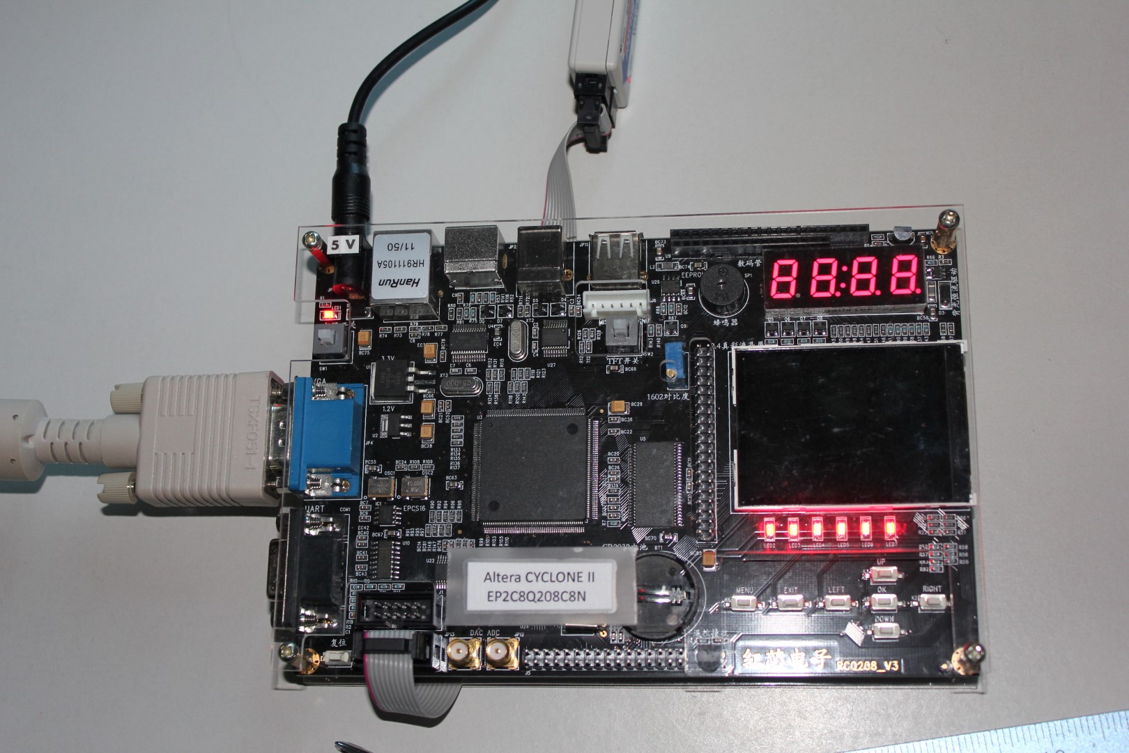
There are many different engineering or experimental FPGA boards that you can get. Each FPGA vendor has a lineup of their own and they can be quite pricey. I purchased mine on eBay from a Chinese seller. They made a board with a plethora of peripherals. Documentation was not great; many things were written in Chinese. I had to copy & paste to Google Translate to get some of the details out of it. However, the price was right!
This is a board that I got. It is marked as “RedCore”:
After a little bit of experimentation and cramming to learn some Verilog, I set about creating a simple project of having it display some text on a VGA monitor.
The overall design was done in Altera Quartus II software. The top-level code was made through a block diagram (schematic). Several blocks were imported from the rich Quartus software support library. Finally, two critical modules that actually bind those pieces into a cohesive implementation were custom-written in Verilog.
Here is the top-level diagram with annotations (click to enlarge):
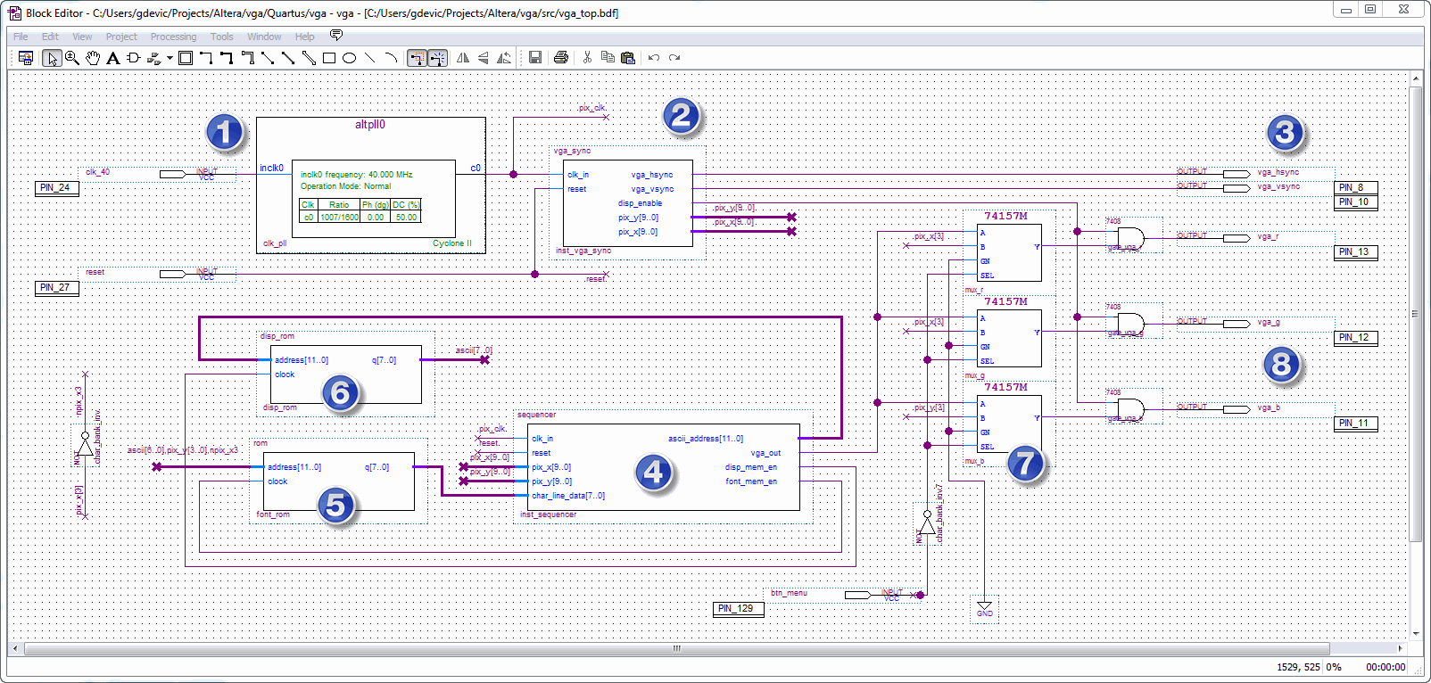
The numbers in blue follow the flow:
- Input pin 24 is connected to a 40 MHz crystal oscillator which is on the board outside the FPGA chip. This frequency is fed into a PLL that is generating 21.175 MHz. That is the required pixel clock for a 640×480 VGA mode I wanted to use.
- The pixel clock is fed into the vga_sync custom module written in Verilog. This module literally counts pixel clocks and generates VGA synchronization pulses. VGA standard is not too difficult to implement: everything is a multiple of pixel clock. Here is the actual Verilog code implementing this module:
// Module VGA_SYNC // // Generates output sync signals to drive VGA display in 640x480 pixel mode: // // Refresh rate: 60 Hz // Vert. refresh: 31.46 kHz // Pixel frequency: 25.175 MHz // // Horizontal timing (pixels) Vertical timing (pixels) // Visible area: 640 480 // Front porch: 16 10 // Sync pulse: 96 2 // Back porch: 48 33 // Whole line: 800 525 module vga_sync ( input clk_in, // Input 25.175 MHz clock, this is a pixel clock for this VGA mode input reset, // Input async. active low reset signal output reg vga_hsync, // Output horizontal sync signal output reg vga_vsync, // Output vertical sync signal output reg disp_enable, // Set when a writable portion of display is enabled: output reg[9:0] pix_x, // x-coordinate of an active pixel output reg[9:0] pix_y // y-coordinate of an active pixel ); //====================================================================== localparam SYNC_ON = 1'b0; // Define the polarity of sync pulses localparam SYNC_OFF = 1'b1; reg[9:0] line_count; // Line counter, current line reg[9:0] pix_count; // Pixel counter, current pixel always @( posedge clk_in or negedge reset ) begin if (!reset) begin line_count <= 0; // On a reset, restart counters from 0 pix_count <= 0; end else begin pix_count <= pix_count + 1;// Increment a pixel counter every clock time! // This is a state machine based on a pixel count. Since VGA modes timings are // based on a multiple of pixel counts, we add them up and generate syncs at // proper times case (pix_count) 0: vga_hsync <= SYNC_OFF; 16: vga_hsync <= SYNC_ON; 112: vga_hsync <= SYNC_OFF; 800: begin line_count <= line_count + 1; pix_count <= 0; end endcase // Properly toggle vertical sync based on the current line count case (line_count) 0: vga_vsync <= SYNC_OFF; 10: vga_vsync <= SYNC_ON; 12: vga_vsync <= SYNC_OFF; 525: begin line_count <= 0; end endcase // The following code defines a drawable display region and outputs // disp_enable to 1 when within that region. Also, set the pixel coordinates // (normalized to the top-left edge of a drawable region) disp_enable <= 0; pix_x <= 0; pix_y <= 0; if (line_count>=35 && line_count<515) begin if (pix_count>=160 && pix_count<800) begin disp_enable <= 1; pix_x <= pix_count - 10'd160; pix_y <= line_count - 10'd35; end end end end endmodule - The vertical and horizontal synchronization pulses are output to appropriate pins. These pins (as well as RGB out) are hard coded to the VGA connector on the board.
- This module, “sequencer” is orchestrating all the action. It will be easier to understand it if I explain the rest of the flow first.
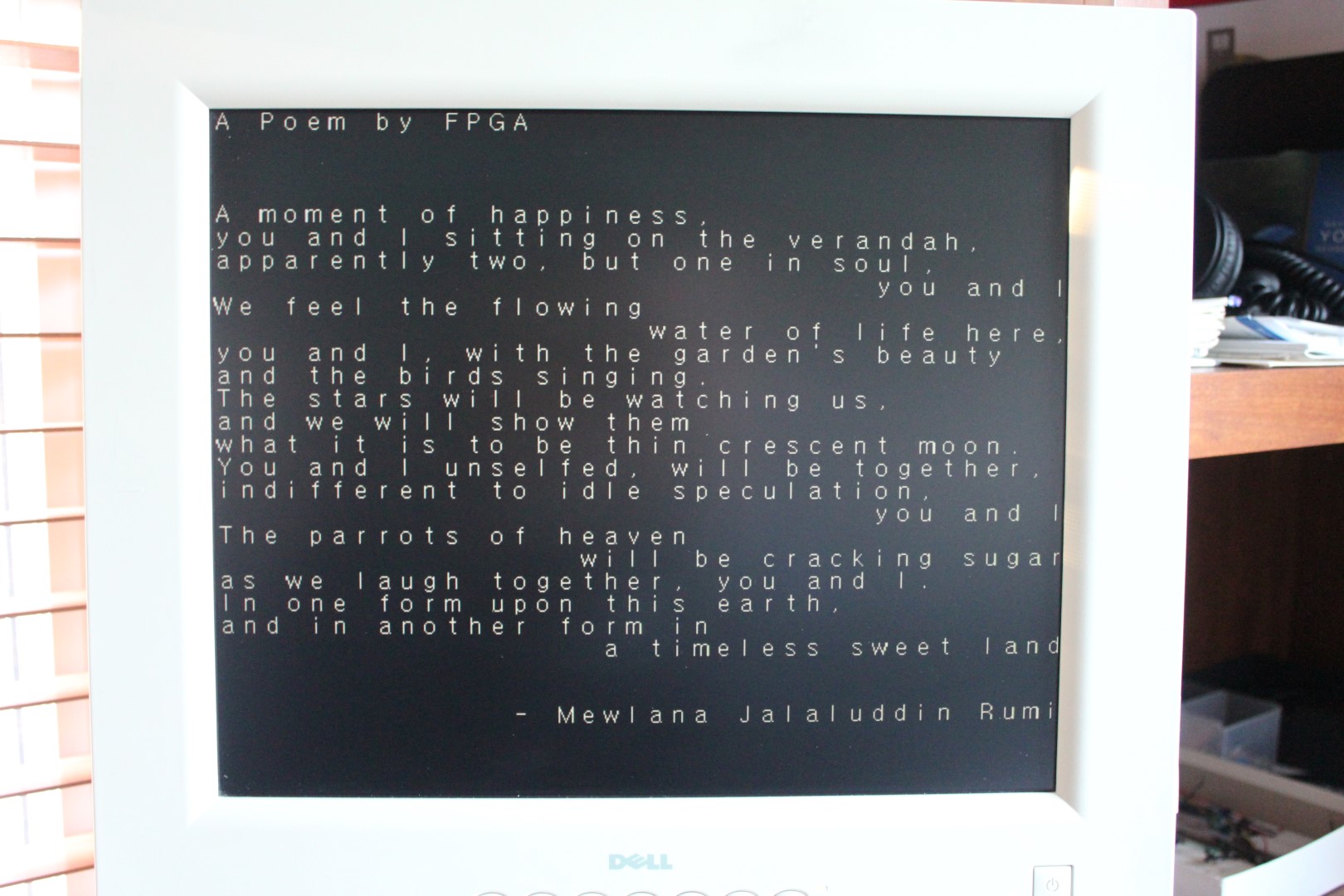
- This is the “display buffer” implemented as ROM. Normally, display buffers use RAM memory (so they can be modified), but I used ROM since I just wanted to display a single static page of text. The memory content of this ROM is set to ASCII text to be displayed. Each line is 40 characters wide, so there are 30 lines with the text that looks like this:
A Poem by FPGA

A moment of happiness,
you and I sitting on the verandah,
apparently two, but one in soul,
you and I
We feel the flowing
water of life here,
you and I, with the garden's beauty
and the birds singing.
The stars will be watching us,
and we will show them
what it is to be thin crescent moon.
You and I unselfed, will be together,
indifferent to idle speculation,
you and I
The parrots of heaven
will be cracking sugar
as we laugh together, you and I.
In one form upon this earth,
and in another form in
a timeless sweet land

- Mewlana Jalaluddin Rumi
- This is the “character ROM”. It contains font definition for each ASCII character. The size of the font used is 16×16 pixels which translates to 16 bit wide x 16 lines, or 2 bytes x 16, or 32 bytes per character. I will explain how I compiled the font later. Sequencer sends a current pixel address scaled down to address individual character in the display memory. Display memory outputs the ASCII character at that location into the font ROM, which in turn returns that character shape back to the sequencer. It then simply shifts it out through its own vga_out port, 8 times for each byte. This repeats every 8 pixels, every line of display.
- This mux is a bypass for the text image. If a button (“btn_menu”, pin 129) is pressed, this part will select a color from a pixel clock instead and will display a colorful pattern. It can be used to test timings without having the rest of the font stuff working.
- Finally, the RGB wires are gated by a display enable signal which is set active only during a time when VGA outputs the text and not a blanking period.
Sequencer is the most complicated Verilog block in this design.
// Module SEQUENCER
//
// Sequences the ASCII character data from display ROM, through the font ROM, and out
// as a monochrome wire data

module sequencer (

input clk_in,                    // Input 25.175 MHz clock, this is a pixel clock for this VGA mode
input reset,                     // Input async. active low reset signal

input [9:0] pix_x,               // The exact X coordinate of a pixel that is currently being drawn
input [9:0] pix_y,               // The exact Y coordinate of a pixel that is currently being drawn

output reg[11:0] ascii_address,  // Address into memory containing a current character code
input [7:0] char_line_data,      // Currect character single line data (8 bit at a time)

output reg vga_out,              // Final VGA out signal (monochrome)

output reg disp_mem_en,          // Enable display memory to read
output reg font_mem_en           // Enable font memory to read
);

//======================================================================

reg [7:0] line_data;             // Current character line data shifter
reg [11:0] xp;                   // Temp
reg [11:0] yp;                   // Temp

always @( posedge clk_in or negedge reset )
begin
   if (!reset) begin
      line_data <= 0;            // Do a mandatory reset of all registers
      ascii_address <= 0;
      disp_mem_en <= 0;
      font_mem_en <= 0;
   end else begin
      ascii_address <= 0;
      // The sequence of getting a pixel to display is clocked by pix_x[2:0]
      // Font it 16x16 pixels, that is two 8-bit words for each line
      case (pix_x[2:0])
         // State 1: send the address of a character to pick up onto the
         //          address bus of the display ROM. Enable both memories
         //          so the output of the first one propagates to the second one
         //          and make it output a line of character definition
         3'b110:  begin
               // Calculate the address within the display memory of a current
               // character based on the current pixel X and Y coordinates
               // There are 40 chars/line, hence multiply Y by 40
               xp[11:0] <= { 6'd0, pix_x[9:4] };
               yp[11:0] <= { 6'd0, pix_y[9:4] };
               ascii_address[11:0] <= (yp << 5) + (yp << 3) + xp;
               //ascii_address[11:0] <= xp + yp * 40;

               disp_mem_en <= 1;
               font_mem_en <= 1;
            end
         // State 2: At this time clock the outputs of both memories should have
         //          stabilized and we can read a line of character definition
         3'b111:  begin
               line_data <= char_line_data;
            end
         // State 3: This is timed to coencide with pix'000 when a new character
         //          line is going to be displayed (@always loop below).
         //          Disable outputs of display and font memories for now
         3'b000:  begin
               font_mem_en <= 0;
               disp_mem_en <= 0;
            end
      endcase
   end
end

always @( posedge clk_in )
begin
   // Depending on the position of a current character pixel, display individual pixels
   // using a buffer that was loaded in a state machine (@always loop above)
   case (pix_x[2:0])
      3'b000:  vga_out <= line_data[7];
      3'b001:  vga_out <= line_data[6];
      3'b010:  vga_out <= line_data[5];
      3'b011:  vga_out <= line_data[4];
      3'b100:  vga_out <= line_data[3];
      3'b101:  vga_out <= line_data[2];
      3'b110:  vga_out <= line_data[1];
      3'b111:  vga_out <= line_data[0];
      endcase
end

endmodule
Still, it should be easy to conceptualize if you carefully read the comments in the code.
Getting the right font was a bit of a separate task with its own challenge. I needed a 16×16 font to divide it nicely into 640×480 pixel resolution. I wanted to use an existing font and not create my own. I also needed to import it as an Intel HEX file in a specific binary format so that my sequencer engine would understand it.
After some experimentation, I settled with a program called Bitmap Font Builder which could load any font from your system and save it as a RAW file (a simple monochrome bitmap without a header). Then I wrote a small utility to read this RAW format and write out a binary file consisting of font data in the particular format I needed. The last step is to have it in Intel HEX file format which Quartus could read when generating the font ROM instance. I used the excellent Hex Workshop editor program to read binary files and export them as Intel HEX.
The process seems a bit convoluted, but it is done only once to generate a font file.
This is the source of my utility to read bitmap and write out the binary font file (click to expand):
/******************************************************************************
*   Date:       2014-01-18                                                    *
*   Copyright (c) 2014 Goran Devic                                            *
*                                                                             *
*   This program is free software; you can redistribute it and/or modify      *
*   it under the terms of the GNU General Public License as published by      *
*   the Free Software Foundation; either version 2 of the License, or         *
*   (at your option) any later version.                                       *
*                                                                             *
*   This program is distributed in the hope that it will be useful,           *
*   but WITHOUT ANY WARRANTY; without even the implied warranty of            *
*   MERCHANTABILITY or FITNESS FOR A PARTICULAR PURPOSE.  See the             *
*   GNU General Public License for more details.                              *
*                                                                             *
*   You should have received a copy of the GNU General Public License         *
*   along with this program; if not, write to the Free Software               *
*   Foundation, Inc., 59 Temple Place, Suite 330, Boston, MA 02111-1307 USA   *
*                                                                             *
*******************************************************************************

    Program Description:

        This tool reads in a bitmap containing a font generated by "Bitmap Font Builder"
        http://www.lmnopc.com/bitmapfontbuilder/ and creates a flat font data file
        suitable to load into a ROM

*******************************************************************************
*   Include Files                                                             *
******************************************************************************/
#include <stdio.h>
#include <stdlib.h>
#include <string.h>

typedef unsigned char BYTE;

long getFileSize(FILE *file)
{
    long lCurPos, lEndPos;
    lCurPos = ftell(file);
    fseek(file, 0, 2);
    lEndPos = ftell(file);
    fseek(file, lCurPos, 0);
    return lEndPos;
}

/******************************************************************************
*   Usage: font_correct font_bitmap.raw > out.txt
*
*   - Minimal error checking
*   - You probably want to recompile to process different bitmap sizes
******************************************************************************/
int main(int argc, const char *argv[])
{
    if (argc==1)
    {
        printf("Usage: font_correct font_bitmap.raw > out.txt\n");
        exit(-1);
    }
    const char *filePath = argv[1];
    BYTE *fileBuf;
    FILE *file;

    if ((file = fopen(filePath, "rb")) == NULL)
    {
        printf("Could not open specified file: %s\n", filePath);
        exit(-1);
    }
    long fileSize = getFileSize(file);

    printf("Source file: %s\n", filePath);
    printf("Size: %d bytes\n\n", fileSize);

    // Read a file into the internal BYTE buffer
    fileBuf = new BYTE[fileSize];

    fread(fileBuf, fileSize, 1, file);
    fclose(file);

    // Generate output file name by modifying the input name
    char outPath[256];
    strcpy(outPath, filePath);
    strcat(outPath, ".dat");
    FILE *fout = NULL;
    if ((fout = fopen(outPath, "wb"))==NULL)
    {
        printf("Could not open output file: %s\n", filePath);
        exit(-1);
    }
    printf("Output file: %s\n", outPath);

    // Define source character bitmap and the destination format
    const int max_ascii = 128;          // Last ASCII code to process
    const int size_y = 16;              // Number of lines (Y) of each character
    const int size_x = 16;              // Number of pixels (X) of each line: 8 or 16
    const int src_num_chars_x = 16;     // Number of characters in one line in the source
    const int src_stride = 256;         // Source stride in bytes from one line to the next

    bool dump = true;

    // Algorithm specific to 512x512 bitmap font square
    for(int ascii=0; ascii < max_ascii; ascii++)
    {
        // Calculate coordinate of each ascii character into the bitmap
        int xc = ascii % src_num_chars_x;
        int yc = ascii / src_num_chars_x;

        dump && printf("---- ASCII 0x%02X '%c'----\n", ascii, ascii>=' '? ascii : ' ');

        // For each horizontal line of that character...
        for(int y=0; y < size_y; y++)
        {
            long outData = 0;           // Contains final character line data

            // For each pixel within that line...
            for(int x=0; x < size_x; x++)
            {
                BYTE bit = fileBuf[ yc*size_y*src_stride + y*src_stride +
                                    xc*size_x + x ];
                if (bit) outData |= 1;
                outData <<= 1;

                dump && printf("%c", bit? '*':' ');
            }

            // Write out a line of character data
            fwrite((const void*) &outData, 1, (size_t) size_x/8, fout);

            dump && printf("\n");
        }
    }
    fclose(fout);

    return 0;
}
Finally, here is an image of A Poem by FPGA:
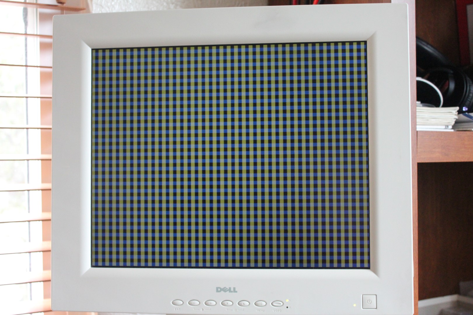
If you press a MENU button on the board, a set of bypass MUXes select the alternative color sources (from the pixel counters) and display this test pattern:
Thank you for you amazing article…
Your work is helping me a lot and I would like to contribute to improve it even more, if you want!
I found a small problem in font_correct.cpp, in the following line:
120 outData <<= 1;
When X = 7, should not cause a left shift. Only the first seven bits.
As your raw character have an edge, its not a problem, however they are rolled to the left… I my case, some characters have all eight bits and don't have edge (something like this: 01010101,10101010,01010101,etc…) and in this case, its a problem for your algorithm.
I suggest you use the following line instead of the current:
120 if (x<size_x-1) outData <<= 1;
Thank you and best regards,
(and sorry-me about my poor English)
Ricardo
Thank you so so much
Hello Goran Devic ,
I have since short a DE1 Board of Altera and try my prgrogrammieren with Verilog teach themselves using examples from the WEB . Could you with posting on their site to complete the project the code for ROM modules yet .
Thank you for this program