In the first post, I described the sequencer, a circuit that provided discrete timing signals to space operations apart. In the second post, I mentioned the Timing matrix that was run by these signals and orchestrated the dance of control signals in time.
This article is about making it all alive and kicking within an FPGA solution.
To make that happen, we need to design a simple “board” that contains our CPU, add some ROM (to hold the boot code), RAM (for the stack), and, well, let’s pick a UART as the simplest IO we can implement and to let the design expresses itself through it!
This project is hosted on GitHub: https://github.com/gdevic/A-Z80.
It is also published on OpenCores: https://opencores.org/project,a-z80
You can download it and start reading the project’s QuickStart document or the User’s Guide.
The folder “host” contains a definition of a board described here.
The folder “tools/zmac” contains Z80 assembly-level code to run. In this case, we will run a test program that will print “Hello, World!” through the UART and using a simple CP/M software interface.
This is a host FPGA board that I was using:
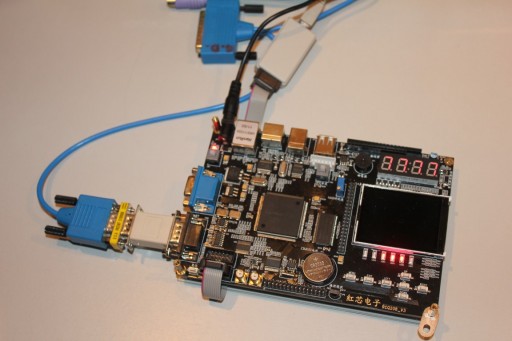
Update: I have switched to using the Altera DE-1 board since the FPGA board shown above was missing the external static RAM memory. SRAM is very simple to use and needs no controller code as the SDRAM does; it is a crucial component if you want to implement a retro computer such as Sinclair ZX Spectrum.
After creating and compiling a design “board”, I tested the external CPU pins using a logic analyzer. By exporting selected pins through the GPIO header I could check various signals, internal and external:
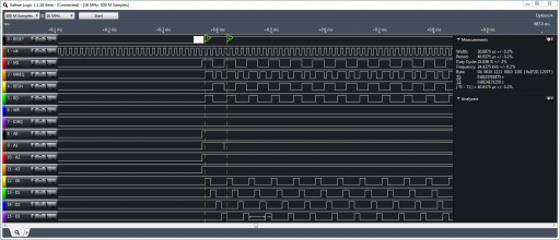
After several rounds of practical improvements – for example, adding a reset button, de-bouncing it, and slowing the clock down so my logic analyzer can capture signals – the FPGA was still behaving strangely.
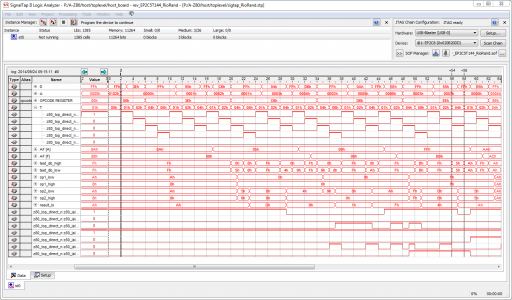
Then, I “discovered” SignalTap – a logic analyzer that is part of the Quartus suite and regretted the time I wasted with hardware probes. SignalTap can do just that – tap into a number of internal signals and show you what’s going on. In the image below, you can see T-clocks advancing, opcode register (IR) holding a current instruction, and busses passing values:
Just around that time I also discovered (in horror!) that my design (which was based on latches), while having worked flawlessly on ModelSim, is totally messed up on FPGA due to the timing differences. I had never performed a gate-level simulation, only the RTL. (Hardware folks are now rolling their eyes at us software guys learning the ropes, the hard way…)
The FPGA timings are very unpredictable when you are trying to use latches: the synthesis tool routes signals by its own algorithms and there are delays that make control T-cycles and clocks overlap in strange ways. In contrast to custom ASIC, you can’t simply add gate delays and count on them. A latch would close on the next clock and then store a wrong value, and so on. RTL simulation would not show any of that. So, I went back to the drawing board.
Luckily, it turned out that only a handful of blocks needed to be modified: the address latch, data gates, and a couple of others. In general, I switched from using latches to edge-triggered flops for most internal flags and memory cell bits. I don’t know how well will that compare to the real Z80 once it is better understood, but for now – this design works.
Update: I ended up porting all latches to flops and then fully constraining the design (using the SDC files). With that done, the timings were fully met and the design became very stable.
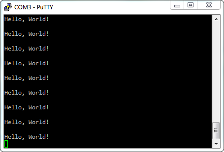
Here is, at last, a “Hello, World!” on a terminal!
I loaded and run “ZEXDOC” and “ZEXALL” test programs that exercised Z80 instructions. All documented and undocumented instructions are passing but only the quirky undocumented CPIR and LDIR family’s IX and IY flags are not correct. This presents no practical problems with any code.
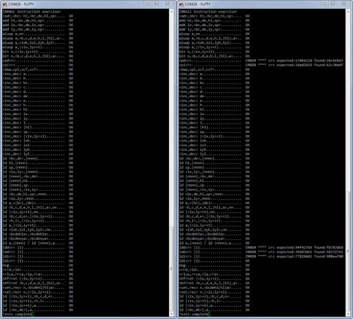
A-Z80 CPU is alive and kicking; created from the gates and schematics – the old school! 🙂
[…] The Soul […]