


This set of short articles will show you the making of a PCB, from the initial requirement stage, through the design and manufacture, and to final software programming.
If you are new to PCB making, I am hoping this text should paint some basic picture of what is involved in a home board design and manufacture. If you are already an experienced hobbyist, I hope you will find some parts informative or interesting enough to try them yourself on your next project. If you see anything wrong or have a better way of doing it, please post it in a comment. I will appreciate learning from you and sharing the experience!
The articles are by no means complete; I did not take as many pictures as I should have or document all the details and problems along the way, but I hope I touched all major parts of that process.
I wanted to explore and learn how to design and make a PCB of moderate complexity at home, without access to specialized labs and equipment, and not use some of the growing numbers of board manufacturing services.
Granted, I do have several specialized instruments (an oscilloscope, a logic analyzer, and my trusted Fluke digital multimeter), but they are all very basic models of their kind and relatively inexpensive. Besides, everyone serious with the hobby of electronics likely already has those.
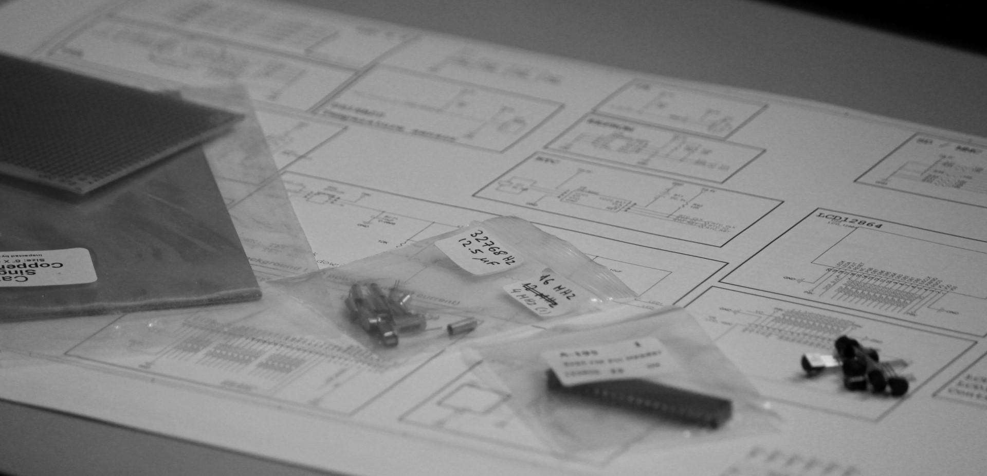
The rest of the equipment used in the process could be considered specialized for home use (CNC drill bits, Dremel tool with a stand, etc.) but it is likely that those, too, could be found in an average garage. If not, they can be purchased in the local hardware store or on eBay for a relatively small price.
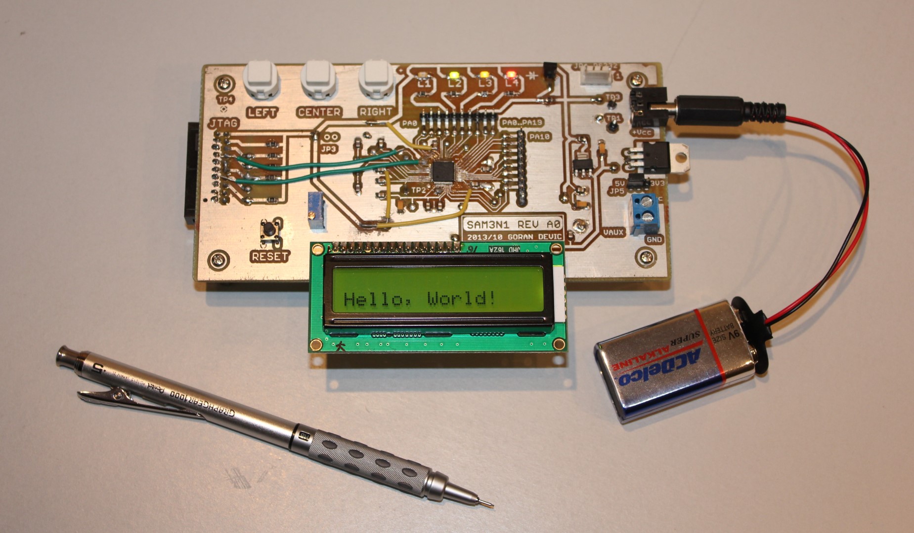
A board that I will be making for this article should touch the limits of what’s doable at home in the DIY (“Do It Yourself”) way. That means using a double-sided and not a simple single-sided PCB. Boards with more than 2 layers (double-sided) cannot be made in a garage. Pushing the limits also meant using SMT components (“Surface-Mount Technology”) over through-hole, where possible.
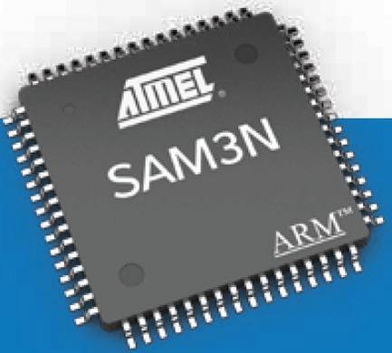
The use of a modern Atmel MCU (“Microcontroller Unit”) also provides a challenging surface-mount pin spacing of 0.5mm. In addition, it is an active device whose ARM core needs to be programmed. That adds the need to tie the board with the software making it very real and contemporary: quite similar designs could be found in many commercial devices around us.
At one point I had to draw a line: I will not do silkscreen or a solder mask with this board. I did not find a reasonably easy and cheap way to do them at home. There are some kits you could buy to photo-etch them, but I think they are expensive and add many steps to the project. If anyone has experience with steps I skipped, please post them.