You can buy or build a special enclosure with a timer and light to expose your boards. Although building it is probably an interesting project unto itself, I’ve found that a cheap desk lamp that I’ve found at a Home Depot discount rack one day, coupled with a simple daylight CFL (“Compact Fluorescent Lamp”) bulb, does the job perfectly. For consistency, I use that lamp (and the bulb) only for this task. Therefore, the bulb has only a few hours of usage and it’s still at its full brightness capacity.
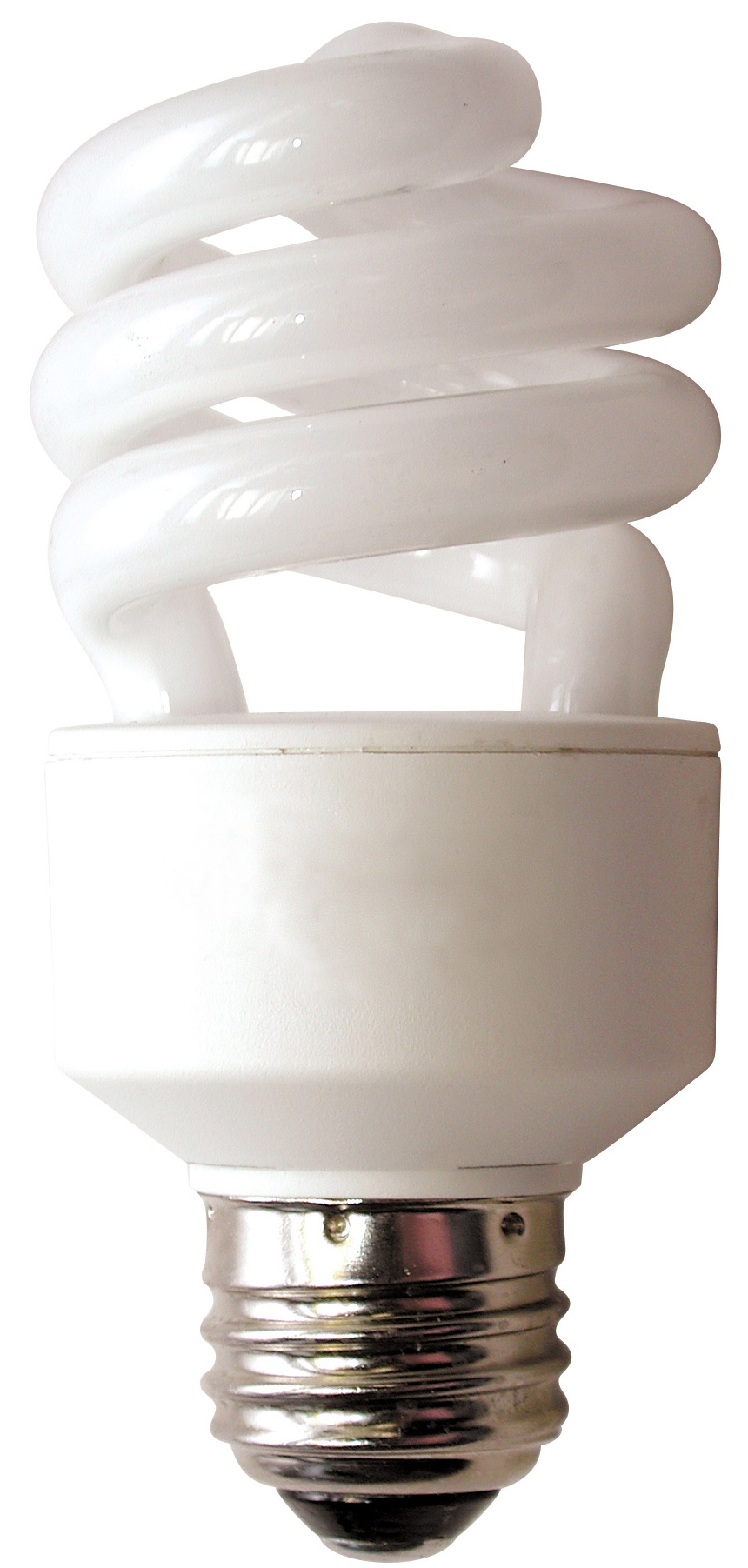
The CFL has to be a wide-spectrum daylight type to emit energy at wavelengths matched to PCB photoresist. Don’t overthink that. Buy a simple “daylight” bulb instead of a specialized bulb and it will work.
When I started using a photoresist, I made one board with various marks and gradually exposed parts of it by pulling a shade over it in one-minute increments. I wanted to find out the efficiency of that CFL bulb and the required exposure. I was surprised to find out just how forgiving that time was: the traces were underexposed to about 4-5 minutes of exposure, and then they were perfect until around 14 minutes where they started showing signs of overexposure.
Since then, I am always using a 10-minute exposure and I am getting consistently good results.
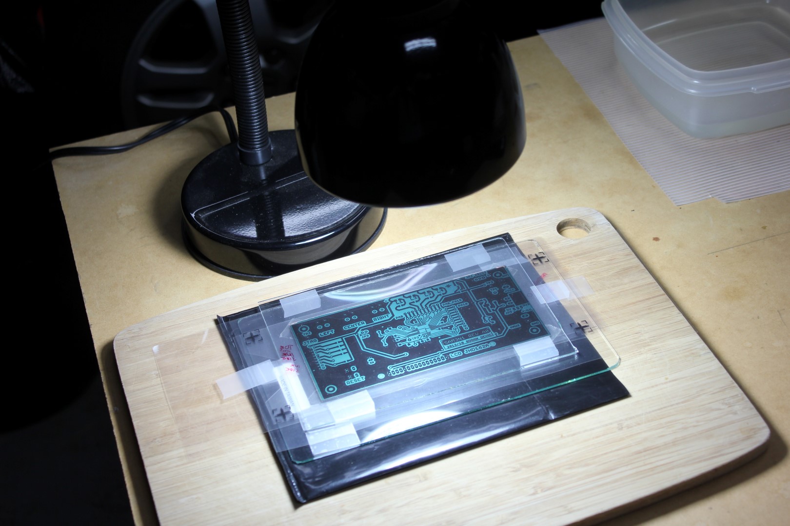
Making a single-layer board is easy: it needs no alignment marks besides those to align double transparency prints for a better black. Make sure to print board outlines to help you position the transparency over the board. Cover it with a glass and expose it for 10 minutes.
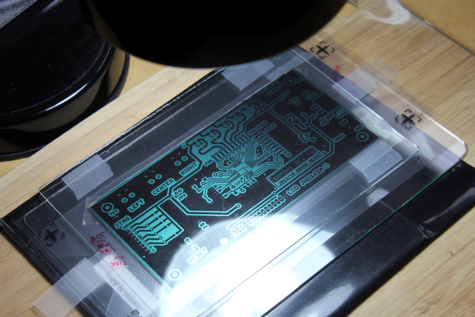
Making a double-side board requires additional layer alignment. When preparing this “sandwich”, time is important: the photosensitive board is exposed while you are taping the foils. I use small pieces of double-sided tapes glued to the corners of a bottom mask; position the board on it which sticks it to the transparency. Then I put a small double tape between the top transparency and the top glass, so by moving the glass I can align the top mask. Then I cover the board and align the top. After exposing the top for 10 min I flip it over (at which point it does not matter if the old top moves) and expose the bottom for 10 min.
Have a developer solution and water containers ready. I am using MG #418 positive developer. It is a liquid and it should be mixed with water in a 1:10 ratio. 500ml bottle will last you a long time. I use a syringe to measure developer and water.
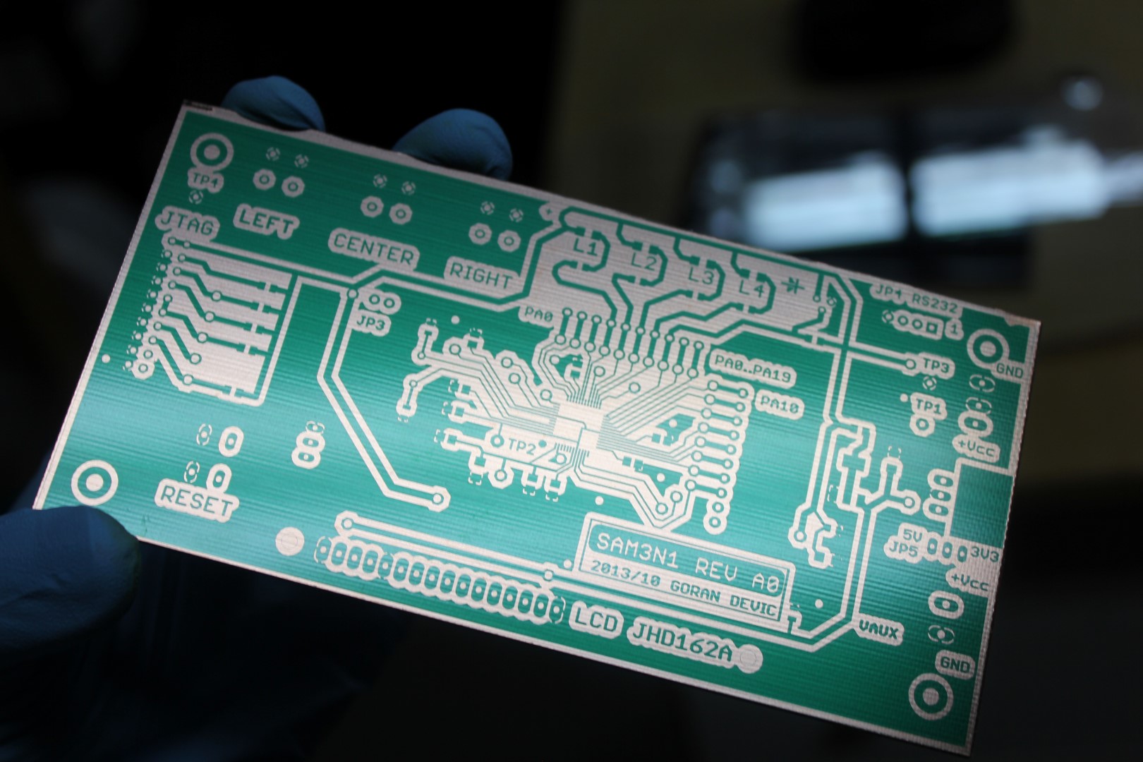
Immediately after CFL light exposure peel off any tape from the corners of the board and dip it into the developer solution. I use a small disposable brush to lightly brush the board and very quickly the traces will be visible. When they are visible and sharp, stop the developing process by rinsing them with plain water (just keep another plastic tray with water next to it). Dry it lightly with a paper towel and store it in the original protective bag – it can stay there; you can etch it later.
Throughout this process, use nitrile gloves at all times. The developer is a strong chemical and it can cause skin irritation. The other reason is that if you can avoid ever touching your board with bare hands you can avoid having to scrub it and clean it later.
Tools: Double-sided tape, single-side tape, lamp to expose, daylight CLF bulb, watch (with a timer), developer, water, disposable foam brush, two plastic containers, syringe (or a measuring cup), nitrile gloves