


When you switch to Eagle’s layout editor, all the components are going to be grouped together in a corner. Yellow lines (“air wires”) will connect pins. A good way to start untangling that mess is to separate and group components that belong to each design block. For example, the power block contains 7805 and a couple of caps and connectors or terminals. Then you can move them around as groups and play with the placement to get a feel of where they would fit on the final board.
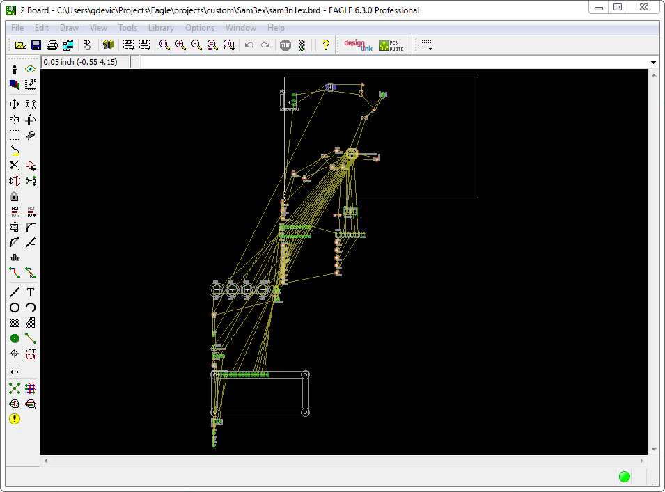
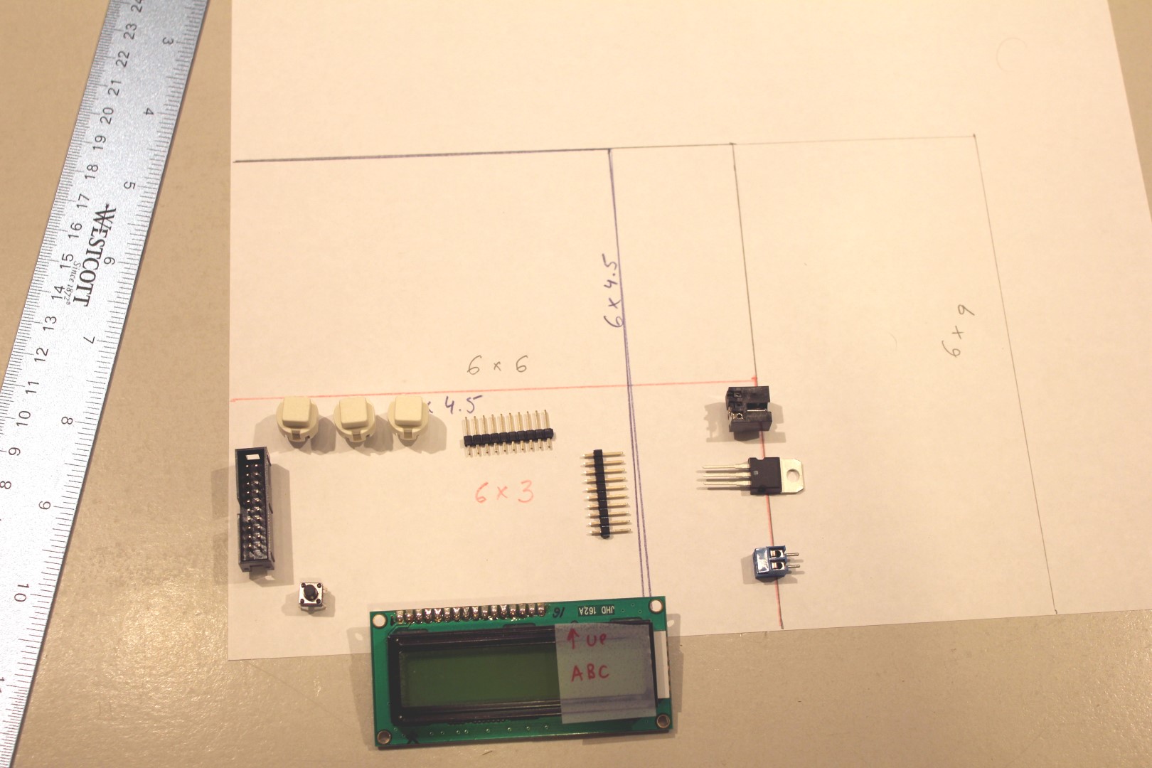
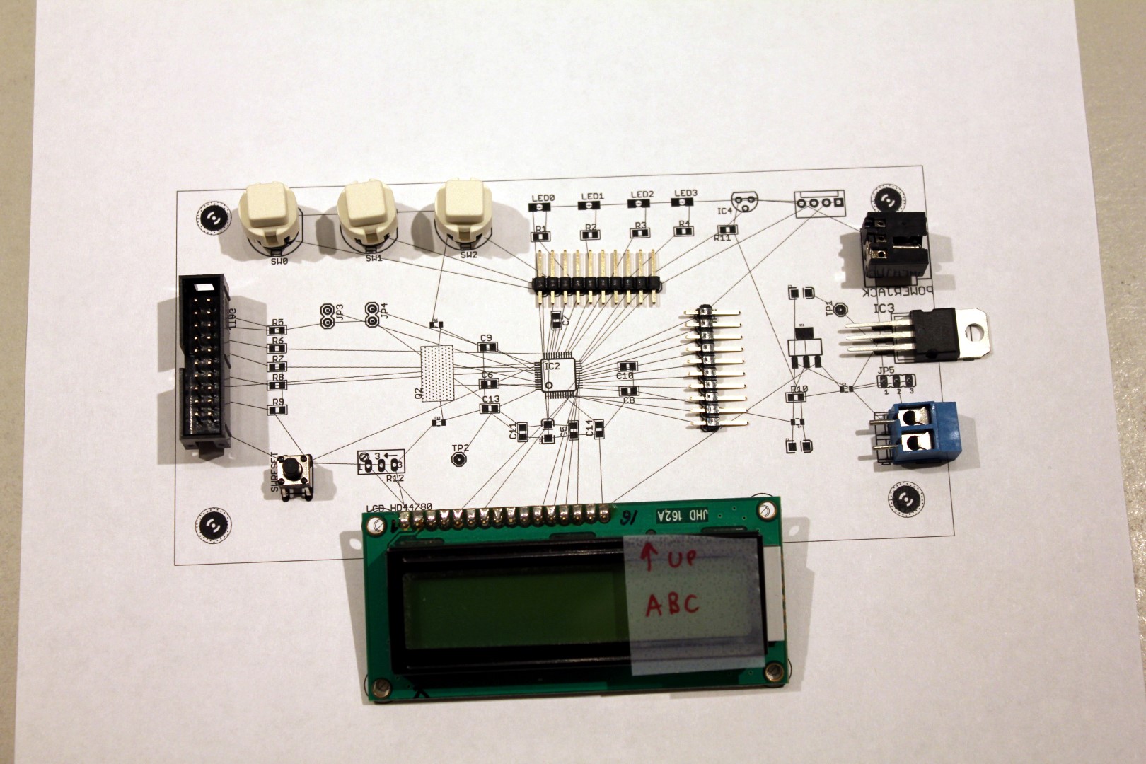
I like to leave the board outlines larger, place parts, and then start shrinking the board until it looks good. The process will depend on your requirement: do you know the final board size? Do you already have an enclosure? Once I had to fit a board in a specific enclosure, so that time I sized it first. For this project, the board could have any size, but I wanted to minimize the cutting: I had a 6×9” PCB and I needed to make just one cut.
These are some standard pre-sensitized PCB sizes:
http://www.circuitspecialists.com/printed-circuit-board-supplies-positive-photo-resist-pre-sensitized-pcbs
Put mounting holes (library: “holes.lbr”)
Assign: Ctrl-E to “ratsnest; move” commands. This is very useful when routing and moving parts.
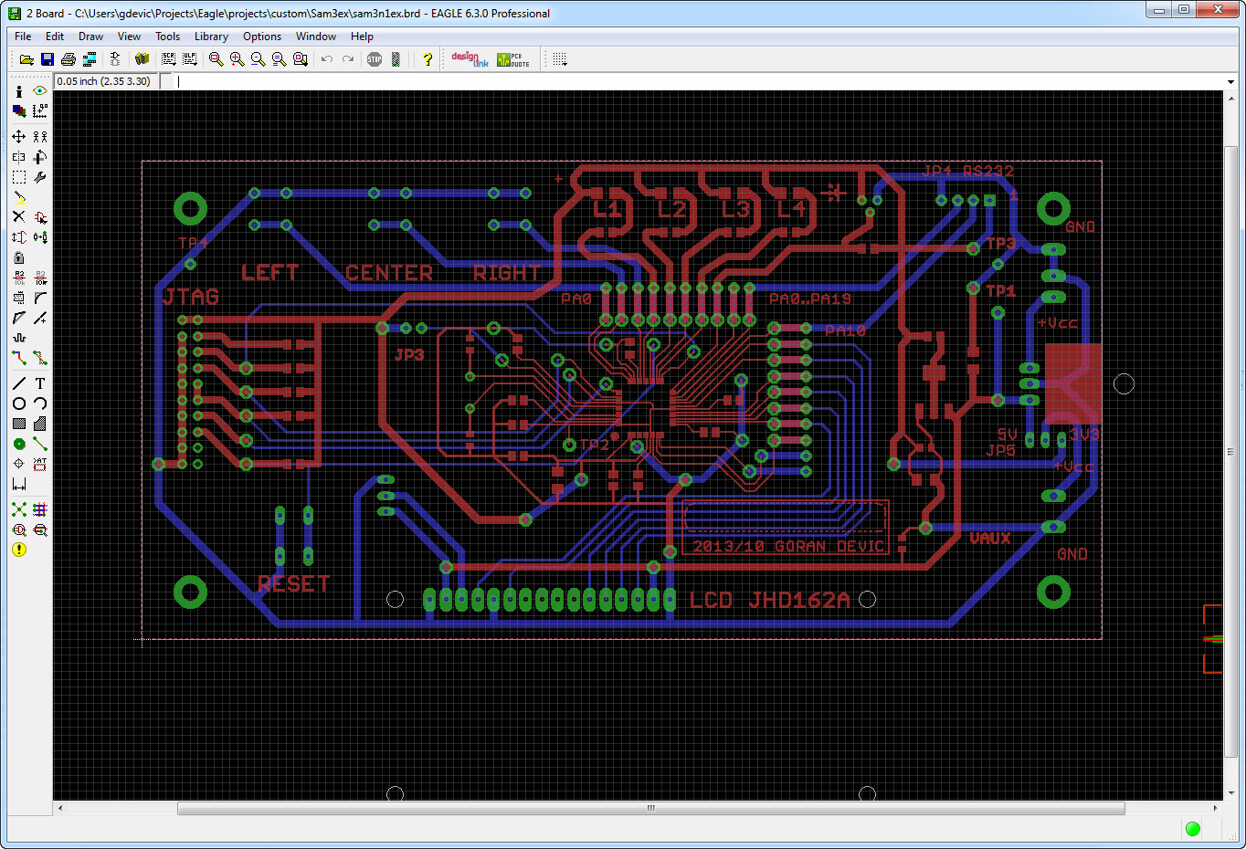
Layout and routing are an art.
You can use Eagle’s auto-router, but I always found I can get better results by manually routing the board. Besides, that is one step in the process that can really make you think hard. It is also a very creative step, so why skip the pleasure by running the auto-router?
Be prepared to keep undoing and re-doing the routing or parts of the routing as you find a progressively better layout.
Run the design rule check on the layout. These rules determine things like pad clearances, line sizes, etc. The default set of Eagle’s design rules may not be the best for your design. You can find the design rule file (extension “dru”) at several places on the web. The one that I like to use came from:
http://dangerousprototypes.com/docs/Get_your_PCBs_made
Lastly, create alignment marks outside the board outline. I like to create these using dedicated layers which I create (101 for “tAlignment” and 102 for “bAlignment”: top and bottom). You will use these marks to align transparencies containing masks.
This step ends the theoretical (and creative) part of the design. The rest is mechanics which can be perfected. I like to intentionally leave a few days of a break at this time: I use it to go over the design and layout with a clear mind. It always amazes me how many problems I only see a day or two later!
Tools: Eagle CAD software