A-Z80 is a conceptual implementation of the venerable Zilog Z80 processor targeted to synthesize and run on a modern FPGA device. It differs from the existing (mostly Verilog) Z80 implementations in that it is designed from the ground up through the schematics and low-level gates.
This design is capable of mimicking the actual Z80 CPU and it illustrates its inner workings for as much as it is known at this time (*).
Introduction
Re-implementing an older, NMOS, and fully custom-designed circuit on a modern FPGA is very challenging and provides a great learning experience to the designer and, hopefully, a design is also very informative and interesting to a curious retro-aficionado as well.
The difference in technology sets some interesting limitations and mandates a certain level of abstraction:
At the lowest level, Z80 uses simple two-transistor latches which are not practical to implement in FPGAs. ASIC flip-flops might be double-edge triggered while the FPGA supports only single-edge triggered; internal Z80 busses are inverted (work nicely with the NMOS logic) while the natural FPGA designs use positive logic; using internal tri-state busses is discouraged in modern FPGA designs; low-level timing characteristic of two technologies are different; it is very difficult to translate timing propagation delays into FPGA where timings might vary greatly depending on the path fitting algorithm has taken etc.
All existing Z80 FPGA implementations that I have seen implement the behavioral model and use Verilog. The most popular and widely used FPGA model is T80. Such models require no deep knowledge of the internal details of a Z80 design since they implement interfaces to higher-level chip blocks (for example, a register file or the ALU). Known undocumented behavior is simply hard-coded within the source.
A-Z80 (this project) implementation strives to be internally structurally identical to the original Z80. Using this approach the model achieves a full cycle accuracy and has identical behavior for all documented and undocumented features not by explicitly hard-coding them but by mimicking the actual design.
This diagram shows the major functional blocks and busses approximately mapped to locations as they appear on a Z80 die.
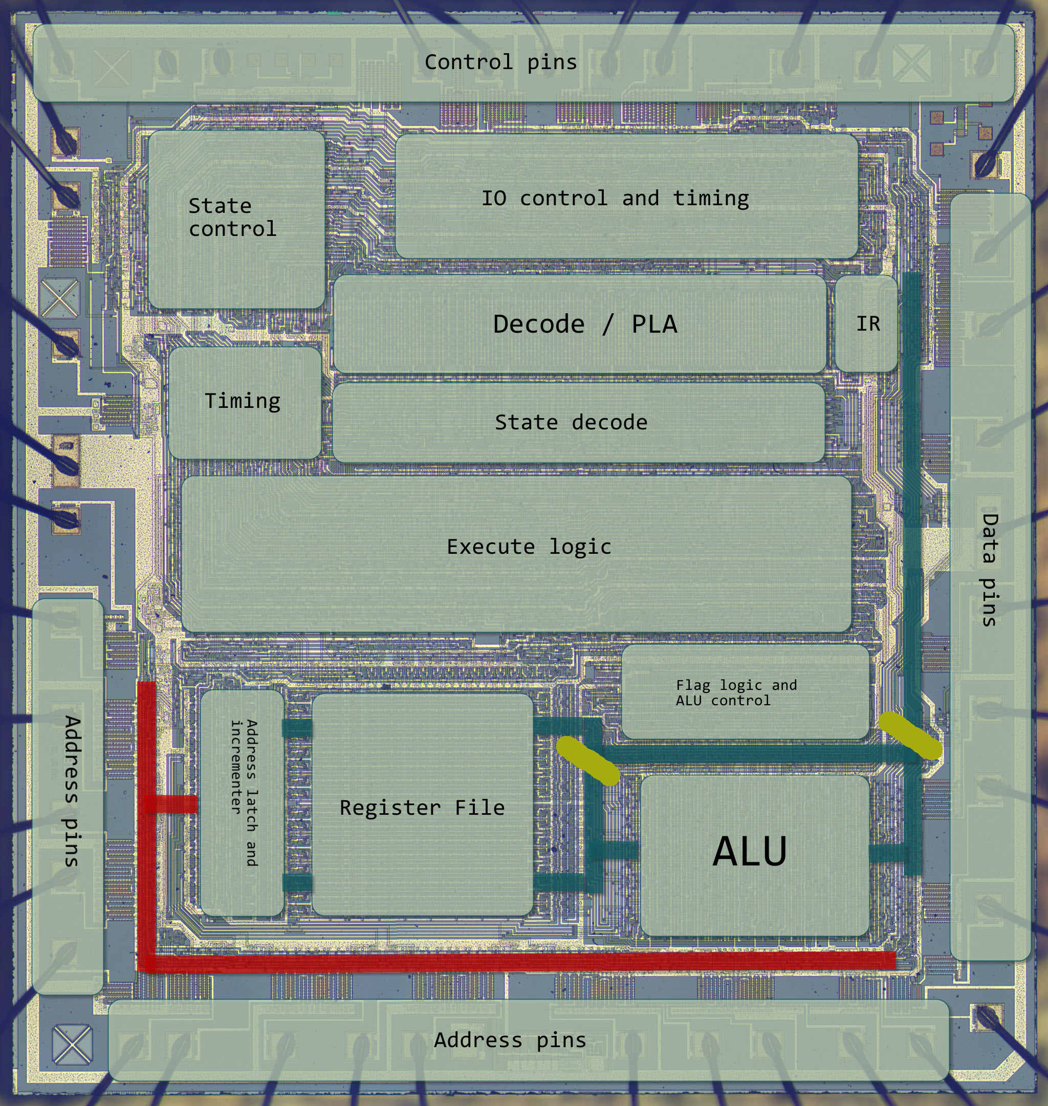
Many details of the internal Z80 architecture are not published and not really known at the time this project was developed (Spring/Summer 2014). A few folks from the Visual6502 team reverse-engineered several blocks from various micro-photographs of a Z80 die. A-Z80 implementation was mainly guided by the reverse-engineering work of Ken Shirriff documented on his Z80 blogs; he provided original schematics of the ALU, register file, address incrementer, and the PLA table. In addition to that, one can pick a lot of details by reading patents, ref-manuals, history museum talks, sources of simulators, previous works of the Z80 designers, etc. Some of these documents are listed in the Library section of this article.
TOP-LEVEL
Conceptually, these are the major Z80 architectural blocks:
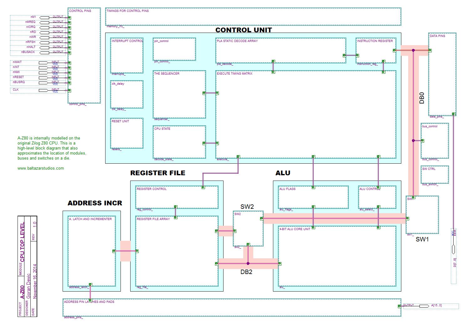
1. Control unit which includes:
- IR (Instruction Register) holds the current instruction that is being executed.
- PLA (Programmable Logic Array) provides static instruction decode.
- The sequencer generates one-hot encoding of M (Machine) and T-cycles which fire in the round-robin fashion and provide timing information for statically decoded instructions. This is “the heart” of the CPU.
- Pin control determines timings for the external CPU pins based on the current function and the T-cycle. Functions are: opcode fetch; memory read, write; IO read, write.
- Interrupts block holds latches and logic for interrupt handing.
- The execute block – the timing matrix – combines M/T timings with statically decoded instructions and fires control signals at precise times.
2. ALU (Arithmetic and Logic Unit) does the number crunching. It includes:
- ALU block proper which is very well described on Ken Shirriff’s blog, please read it.
- Flags contain temporary flag register and the logic to set flags depending on the results of operations.
- A set of various ALU control functions to handle operations such are DAA, parity, rotation selector etc.
3. Register file contains:
- Z80 system and general-purpose registers (AX, BC, …, SP, PC, IR)
- A control unit that selects registers. This is a fairly complex unit since it handles multiple register exchange flip-flops in various addressing modes.
4. Bus is a loose collection of internal bus-related modules:
- Address latch and the incrementer do 16-bit increment/decrement and provide the address for memory/IO addressing. They are well described by Ken on his blogs.
- Data bus switches marked as SW1, SW2, SW4) are used at several places along the data bus to separate segments. They allow multiple parts of the chip to operate at the same time on a single internal data bus.
- Data pins and Address pins implement end-point pads logic connecting the internal buses with the CPU pins.
Several articles that follow this blog describe those components in more detail as implemented in this project. The A-Z80 design is released as open-source and can be downloaded on GitHub: https://github.com/gdevic/A-Z80
The A-Z80 CPU at this stage is a completed, fully working FPGA design. It is applied in a Sinclair ZX Spectrum computer implementation described here. One can use it in Altera or even Xilinx devices since the schematics are compiled into generic Verilog.
Continue reading about The Heart, The Mind, The Soul of this design…
(*) Unbeknownst to me, the Visual 6502 team has made some significant progress reverse-engineering the Z80, during which time I have already made most of the design and improvising/substituting missing parts by designing them “as it would make sense”. This design; however, provides a working foundation that can be modified and aligned to the actual Z80 design as the 6502 team increasingly sheds more light on it.
Hi Goran, been following your work for a while. Congratulations for the results and my admiration for the incredible work. I’m too involved in reverse engineering old school stuff and related very much to your comment about spending a weekend trying to figure out things. hehe
Btw, I posted today something on EDABOARD’s forum, maybe you can have a look and help me. The link: http://www.edaboard.com/thread325474.html
Best regards.
Hi Ed,
I am not that familiar with CMOS, but it does look to be a capacitor. Do you have a complete set of images in high-res? If you presume it’s a cap, does the rest of the circuit make sense?
Thanks!
Hi Goran, it seems that it is a decoupling cap. Just posted another challenge here, have a look: http://www.edaboard.com/thread325534.html
Regards. Ed
Excellent blog post. I certainly appreciate this website. Continue the good work!
I’m looking to create a hardware version of ZEMU, is it possible to use this FPGA version to output the contents of the registers and internal busses so you can step through a ROM and watch what’s going on inside…. A tremendous teaching tool for youngsters
It would probably need a JTAG or some other hardware block that acts as an interface. It would be an interesting exercise to make that.
[…] A Z80 from the Ground Up (2014) 6 by glhaynes | 0 comments on Hacker News. […]
[…] A Z80 from the Ground Up (2014) 6 by glhaynes | 0 comments on Hacker News. […]
[…] http://baltazarstudios.com/z80-ground/ […]